The Comprehensive Guide to High-Density Interconnect (HDI) Boards
In the relentless pursuit of smaller, faster, and more powerful electronics, High-Density Interconnect (HDI) technology has emerged as a critical enabler. This guide delves into the core aspects of High Density Interconnects (HDI) Board, from its fundamental manufacturing processes and material science to application-specific design strategies and supply chain considerations for professionals.
Core HDI Manufacturing: Microvias and Ultra-Fine Lines
The defining capability of HDI boards lies in advanced structures that allow for unprecedented component density and miniaturization.
| Key Technology |
Description and Impact |
| Microvias (Blind/Buried) |
Laser-drilled vias with diameters typically less than 150µm. They connect adjacent layers without passing through the entire board, saving crucial space and enabling more direct routing paths, which is fundamental for complex, compact designs. |
| Ultra-Fine Line Tracing |
The ability to produce trace widths and spacings as fine as 3 mils (0.075mm). This allows for a significantly higher number of connections in a given area, directly supporting the use of advanced, fine-pitch ball grid array (BGA) components. |
| High Aspect Ratio |
The capability to achieve a plate thickness-to-aperture ratio of up to 10:1. This is crucial for reliably plating deep, small-diameter microvias, ensuring electrical connectivity in multi-layer HDI stacks. |
Manufacturers specializing in HDI, such as Anhui Hongxin Electronic Technology Co., Ltd., leverage these technologies to build complex boards ranging from 0.3mm to 6mm in thickness and up to 32 layers, forming the backbone of modern compact devices.
The HDI Development Workflow: From Design to Delivery
Successfully bringing an HDI design to mass production requires navigating a detailed and sequential process.
- Design and Engineering Review: This initial phase is critical. It involves verifying design rules (DRC), planning the layer stack-up, and selecting appropriate materials (e.g., high-Tg FR-4 for thermal reliability). Close collaboration with your manufacturer's engineering team at this stage prevents costly delays.
- Sequential Lamination and Fabrication: HDI boards are built through multiple lamination cycles. A core is fabricated first, followed by successive layers with microvias. Processes like laser drilling, precise copper plating, and pattern imaging are repeated, demanding exceptional process control.
- Testing and Quality Assurance: Given the complexity, electrical testing (including flying probe or fixture-based testing) is mandatory to verify net connectivity and isolation. Impedance control testing is also common for high-speed designs.
Leading manufacturers optimize this workflow to offer competitive lead times. For instance, a structured 25-day production cycle for bulk HDI orders balances thorough manufacturing with time-to-market needs, while rapid 24-hour prototyping services support initial design verification.
Material Selection for HDI Reliability and Performance
The choice of base material and finish directly impacts the functionality, durability, and yield of an HDI board.
- Substrate Materials:
- Standard & High-Tg FR-4: The workhorse for many applications. High-Tg grades are essential for lead-free soldering and operations in higher temperature environments.
- Specialized Laminates: For high-frequency/speed applications (e.g., 5G modules), low-loss materials like Rogers or specialized hydrocarbon ceramics may be integrated into the stack-up.
- Flex and Rigid-Flex Materials: Polyimide films are used in areas requiring bending, enabling innovative form factors in wearables and compact electronics.
- Surface Finishes: The finish must be suitable for fine-pitch components. Immersion Gold (ENIG) offers a flat surface excellent for soldering and wire bonding, while Immersion Silver or advanced OSP formulations provide cost-effective alternatives for specific use cases.
HDI as an Innovation Enabler in Key Industries
HDI technology is not just a PCB type; it is a strategic solution for product innovation.
- 5G Smartphones and Consumer Tech: HDI allows for the extreme miniaturization needed to pack multiple 5G antenna modules, advanced processors, and large batteries into a slim profile. It enables the use of chip-on-board (COB) and package-on-package (PoP) techniques.
- High-Reliability Aerospace and Medical: In these fields, HDI's value is in reliability and performance density. It allows for more functionality in space-constrained avionics boxes or portable medical monitors, often utilizing rigid-flex constructions for durability.
- Advanced Automotive Electronics: As vehicles incorporate more ADAS (Advanced Driver Assistance Systems) and in-vehicle infotainment, HDI boards manage the complex, high-speed networking between sensors, cameras, and control units, often requiring compliance with automotive-grade standards like IATF 16949.
FAQ
What exactly defines a board as an "HDI" PCB?
An HDI PCB is primarily defined by its higher wiring density per unit area compared to traditional PCBs. This is achieved through specific features:
- Microvias: The use of blind and/or buried vias with a diameter typically ≤150µm.
- Finer Lines and Spaces: Trace widths and clearances of 3 mils (0.075mm) or less.
- Higher Connection Pad Density: The ability to accommodate components with very fine pitch (e.g., <0.5mm pitch BGAs).
- Sequential Build-Up Layers: Often involves multiple lamination cycles to create the interconnected layers.
A board incorporating several of these elements, especially microvias, is generally classified as HDI.
When should I consider using an HDI design over a standard multilayer PCB?
You should strongly consider HDI technology when your design faces one or more of these challenges:
- Space Constraints: The product enclosure is very small (e.g., wearable, hearable, ultra-thin smartphone).
- High-Pin-Count Components: You need to route out a modern CPU, FPGA, or memory chip with a fine-pitch BGA footprint.
- High-Signal-Performance Requirements: You need shorter, more direct signal paths for superior electrical performance (e.g., faster speeds, less cross-talk).
- Increased Functionality in Same Size: You need to add significant new features to a product without increasing its PCB footprint.
If your design only uses large-pitch components and has ample board space, a standard multilayer may be more cost-effective.
Why are HDI boards more expensive, and how can I manage costs?
The increased cost stems from:
- Complex Processes: Additional production steps like sequential lamination, laser drilling, and more precise imaging.
- Advanced Equipment: The need for high-precision manufacturing and inspection machinery.
- Lower Yields Initially: The complexity can lead to lower production yields, especially for new or highly complex designs.
Cost Management Strategies:
- Optimize Layer Count: Work with your manufacturer to use the minimum number of layers necessary.
- Simplify Via Structures: Use microvias only where absolutely needed. A "1+N+1" stack-up is less expensive than "any-layer" HDI.
- Design for Manufacturability (DFM): Adhere strictly to the manufacturer's DFM guidelines to prevent yield issues.
- Plan for Volume: Unit cost decreases significantly with higher order quantities due to optimized panel utilization and setup amortization.
What are the key certifications I should look for in an HDI board manufacturer?
Certifications are a proxy for a manufacturer's process control and reliability. The most important ones include:
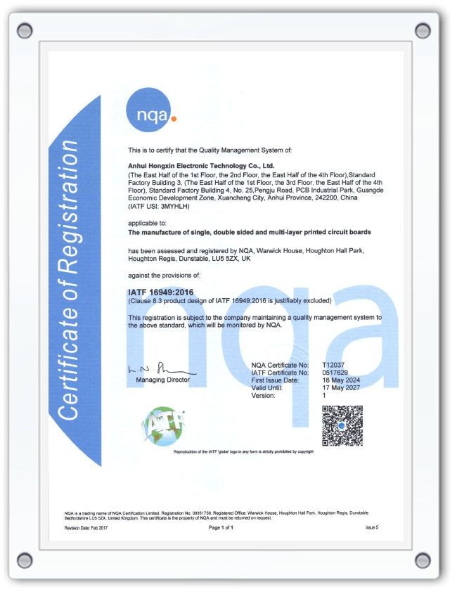
- IATF 16949: The automotive quality management standard. It demonstrates a top-tier commitment to systematic process control, traceability, and continuous improvement—highly valuable even for non-automotive projects.
- ISO 9001: The baseline quality management system certification.
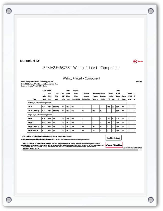
- UL Recognition: Ensures the board materials and construction meet safety standards, often required for end products sold in many regions.
- IPC Standards Compliance: While not a certification, adherence to standards like IPC-6012 (performance) and IPC-6018 (HDI) is a strong indicator of technical capability.
A manufacturer like Anhui Hongxin Electronic Technology Co., Ltd., holding IATF 16949, ISO, and UL certifications, demonstrates a robust framework for producing reliable HDI boards.
How does rapid prototyping for HDI boards work with a 25-day bulk production cycle?
This two-tiered approach is designed to support both innovation and scaling:
- Rapid Prototyping (e.g., 24-72 hours): This service uses expedited scheduling for small panels (often 1-5 pieces). It focuses on design validation—checking electrical connectivity, basic functionality, and fit. It may use slightly relaxed tolerances or different tooling to achieve speed.
- Structured Bulk Production (e.g., 25 days): Once the design is verified, full-scale production begins. This involves finalizing and manufacturing all dedicated tooling (laser drill files, lamination plates, test fixtures), running full DFM checks, and producing the order on large panels with strict process control for optimal yield and consistency. The 25-day cycle encompasses this complete, optimized workflow for volume orders.
This model allows companies to iterate designs quickly without commitment and then transition seamlessly to a reliable, cost-effective volume supply chain.


 English
  Español
  Français