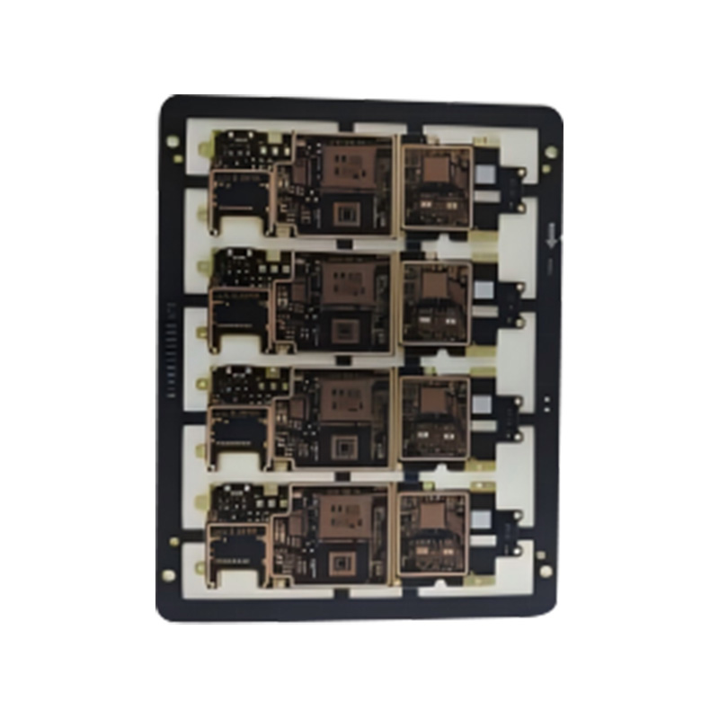
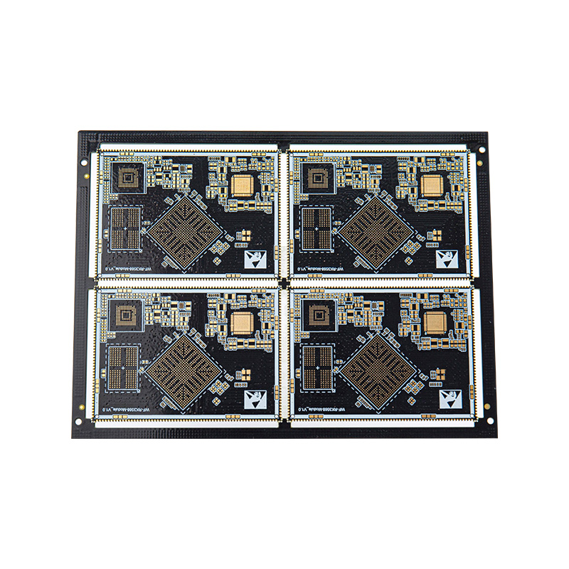
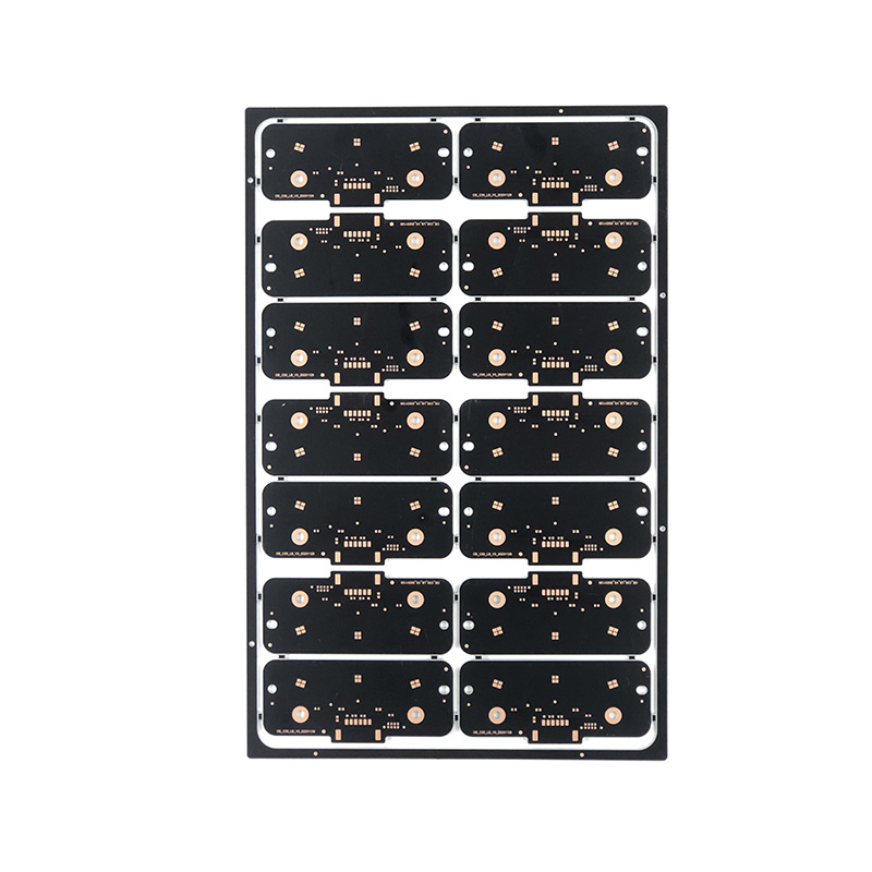
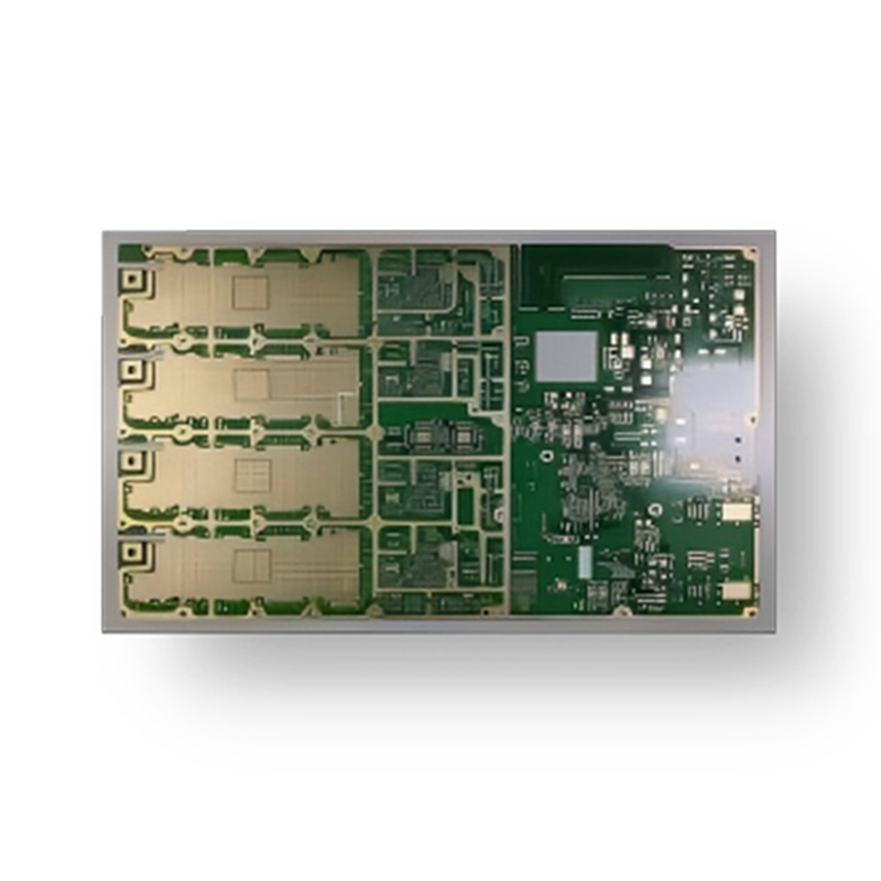
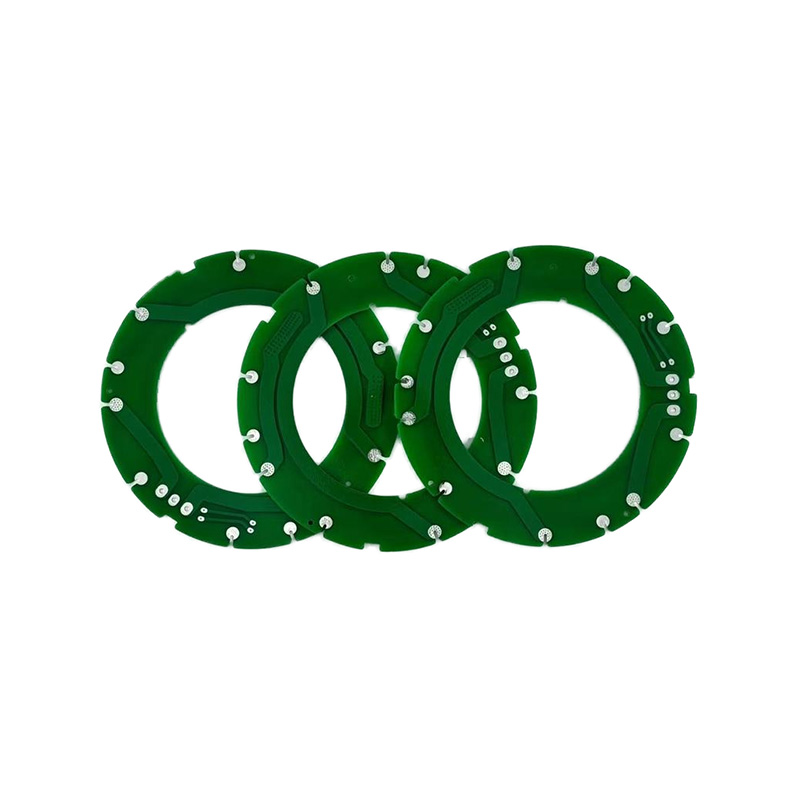
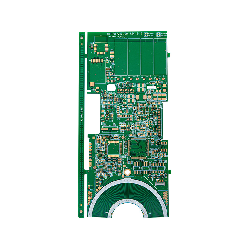
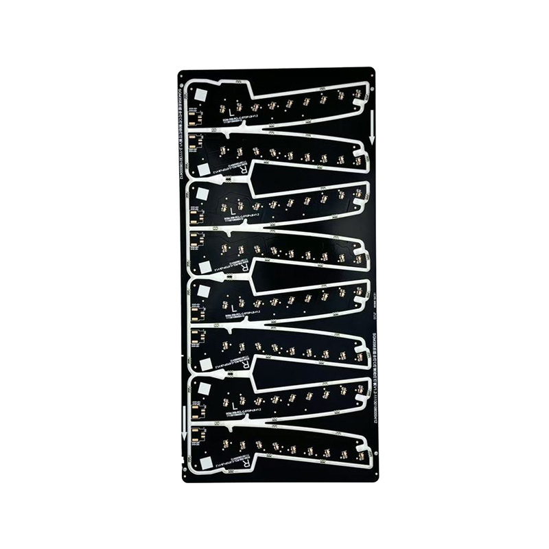
2-Layer 6-Level HDI Board
HDI (High Density Interconnect) PCBs achieve ultra-high wiring density and miniaturized structures through microvias (blind and buried vias), fine lines (line width/spacing ≤75μm), and multi-layer stacking technology, saving over 60% of space compared to traditional PCBs. They utilize laser drilling and electroplating to fill holes, supporting interconnects of more than eight layers and any-layer conduction design. They can accommodate high-end chips with a BGA pitch of 0.3mm and are widely used in compact products such as smartphones, drones, AR/VR devices, and medical microelectronics. HDI boards combine excellent signal integrity and heat dissipation performance, significantly improving the quality of high-frequency signal transmission. They are a core solution for 5G terminals, IoT modules, and other applications that require lightweight, thin, and multifunctional integration. They are particularly suitable for microelectronic systems requiring high precision and reliability.
- Specification
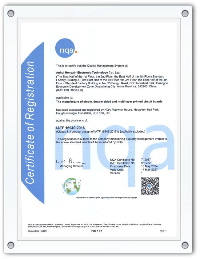
- About Hongxin
- Contact Us
|
Material |
HDI |
|
Board thickness |
0.3-6mm |
|
Copper thickness |
0.5oz-5oz |
|
Layers |
1-32 |
|
Place of origin |
Anhui, China |
|
Surface finish |
Standard HASL, lead-free HASL, OSP, immersion nickel/gold, blue glue, immersion silver, immersion tin |
|
Minimum aperture |
0.25mm |
|
Minimum trace width |
3mil (0.075mm) |
|
Minimum trace spacing |
0.075mm |
|
Board thickness to aperture ratio |
10:1 |


 English
  Español
  Français
