


 English
  Español
  Français
What Is PCB Design? Basics, Steps, Stackup & Troubleshooting Tips
Content
What Is PCB Design?
PCB design is the process of translating an electronic circuit schematic into a physical board layout that can be manufactured. The designer specifies where each component sits, how copper traces connect them, how many layers the board requires, and what materials and tolerances the fabricator must meet. The output is a set of Gerber files — the industry-standard format that drives automated fabrication equipment.
A finished PCB is more than a wiring diagram made permanent. It is a mechanical structure, a thermal management system, and an electromagnetic environment all at once. A well-designed board routes signals cleanly, dissipates heat efficiently, and passes EMC testing. A poorly designed one may function on the bench but fail in the field due to noise, crosstalk, or power integrity issues that only appear under real operating conditions.
Basics of PCB Design Every Engineer Should Know
Before opening any EDA tool, a designer needs to be comfortable with a handful of foundational concepts that govern every decision made during layout.
Layers and Stackup
PCBs consist of alternating copper and dielectric (insulating) layers laminated together. Simple designs use 2 layers; boards with higher component density or stricter signal integrity requirements use 4, 6, 8, or more. Each layer serves a role — signal routing, ground reference, or power distribution — and the arrangement of these layers is called the stackup.
Impedance and Signal Integrity
At high frequencies, a copper trace behaves as a transmission line. Its characteristic impedance — determined by trace width, copper thickness, dielectric constant, and distance to the nearest reference plane — must match the source and load impedance to prevent reflections. Most digital interfaces target 50 Ω single-ended or 100 Ω differential. Deviating from these values causes signal degradation that worsens with frequency.
Return Currents and Reference Planes
Every signal current has a return path. At high frequencies, that return current travels directly beneath the signal trace on the nearest reference plane — not through the shortest DC path. Interrupting this return path, for example by routing a trace across a plane split or a slot, forces the return current to detour and creates a loop antenna that radiates EMI. Keeping reference planes continuous under high-speed routing is one of the most impactful layout decisions a designer makes.
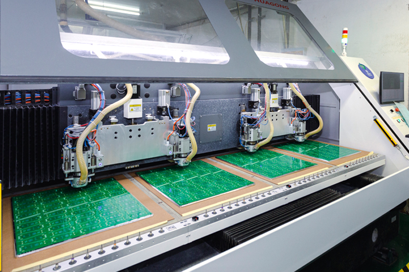
PCB Board Design Steps
The PCB design process follows a consistent sequence regardless of board complexity. Skipping steps — particularly early design reviews — typically results in costly respins.
- Schematic capture: Define all components, net connections, and electrical rules in an EDA tool. Assign footprints to each component symbol.
- Design requirements and constraints: Document board dimensions, layer count, minimum trace/space rules, impedance targets, thermal requirements, and regulatory standards (IPC-2221, IPC-2152, etc.).
- Stackup definition: Choose the layer count, material, dielectric thickness, and copper weight. Confirm impedance targets with your fabricator before routing begins.
- Component placement: Place components to minimize trace lengths for critical nets, group related circuitry, respect thermal zones, and meet mechanical constraints. Placement drives 80% of routing quality.
- Power and ground routing: Route power rails and establish ground planes before signal routing. Decoupling capacitors must sit as close as possible to IC power pins.
- Signal routing: Route high-speed and sensitive signals first, maintaining impedance, minimizing via transitions, and keeping differential pairs coupled and length-matched.
- Design Rule Check (DRC): Run automated checks for clearance violations, unconnected nets, annular ring size, and fabrication constraints.
- Gerber generation and fabrication review: Export manufacturing files and review them in a Gerber viewer before submission. Confirm stackup, drill files, and silkscreen with the fabricator.
6 Layer PCB Stackup Example
A 6 layer stackup is the most practical upgrade from a 4 layer board when a design involves high-speed interfaces, dense BGA routing, or strict EMI requirements. The additional layers allow dedicated reference planes to bracket the inner signal layers, creating a controlled stripline environment that reduces radiation and crosstalk.
A standard 6 layer arrangement for a 1.6 mm FR-4 board:
| Layer | Function | Typical Use |
|---|---|---|
| L1 (Top) | Signal | Component placement, microstrip routing |
| L2 | Ground Plane | Primary reference for L1 and L3 |
| L3 | Signal | High-speed stripline: DDR, USB, PCIe, clocks |
| L4 | Power Plane | Main power distribution |
| L5 | Signal | Control signals, busses, lower-priority nets |
| L6 (Bottom) | Signal | Secondary components, connectors |
With L2 as ground and L4 as power, Layer 3 sits in a true stripline configuration — sandwiched between two reference planes — making it the right home for the most noise-sensitive signals. The thin prepreg between L1 and L2 (typically 3–4 mil) keeps 50 Ω trace widths achievable at around 4–5 mil, compatible with standard fabrication processes.
How to Troubleshoot a PCB
Even well-designed boards occasionally arrive from fabrication with defects, or fail after assembly. A structured troubleshooting process — rather than random component swapping — finds faults faster and avoids collateral damage.
Step 1: Visual Inspection Before Powering On
Under magnification, examine the board for solder bridges on fine-pitch ICs, cold joints (dull and grainy rather than smooth and shiny), missing or reversed components, and any visible trace damage. A significant proportion of assembly defects are visible before any instrument is needed.
Step 2: Power Rail Verification
Before applying full power, measure resistance from each power rail to ground with a multimeter. A low or near-zero reading indicates a short — common causes include solder bridges, damaged capacitors, or a reversed polarized component. Once clear, apply power through a current-limited bench supply set just above expected consumption. A collapsing rail under load points to an overloaded regulator or a shorted downstream component.
Step 3: Signal-Level Diagnosis
With rails confirmed good, use an oscilloscope to check clock signals, reset lines, and communication bus activity. Missing clocks, stuck reset lines, or malformed SPI/I2C/UART waveforms each point to a specific area of failure. A logic analyzer is more efficient than an oscilloscope for capturing multi-signal digital bus behavior over time.
Step 4: Component-Level Testing
If signal tracing isolates a suspected component, in-circuit resistance measurements (with power off) can confirm open or shorted junctions on passives. For ICs, comparing pin voltages against the datasheet's operating conditions table quickly narrows whether the device is receiving correct supply, reference, and enable signals. When a component is confirmed faulty, replace it with a known-good part before drawing conclusions — substituting with another part from the same potentially defective batch solves nothing.
Recommended Products

 LET'S CREATE THE FUTURE TOGETHER

Contact Us Anytime
Copyright © Anhui Hongxin Electronic Technology Co., Ltd. All Rights
Reserved.
privacy
Wholesale Printed Circuit Board Suppliers, Manufacturers

