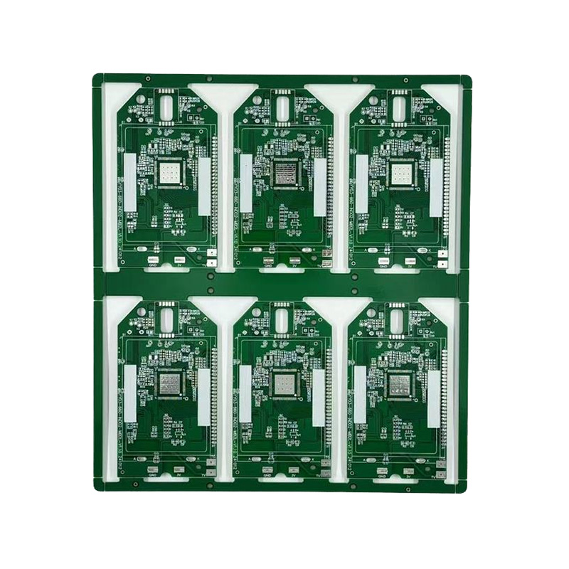
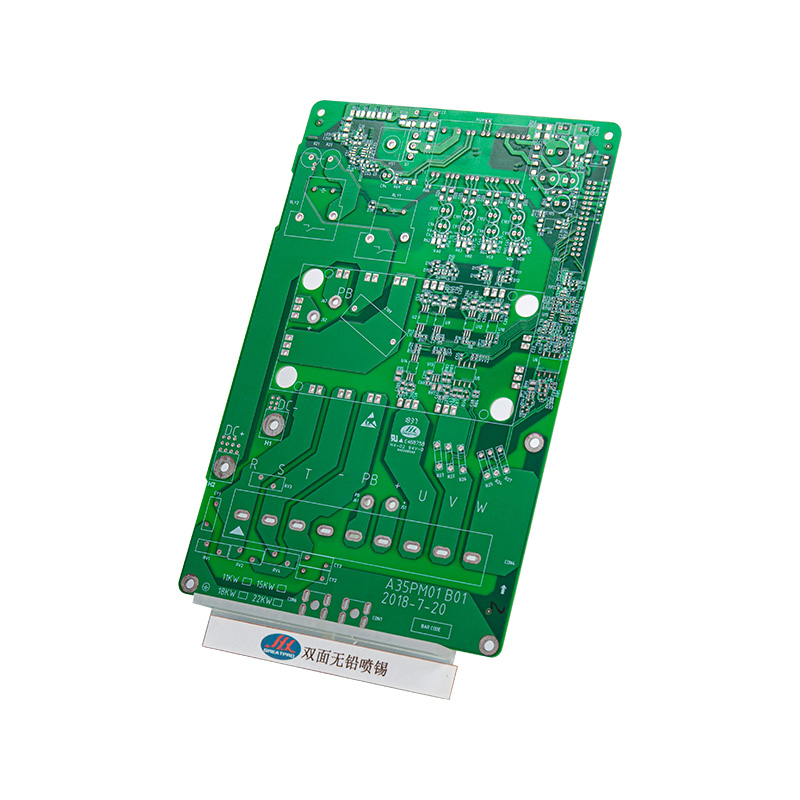
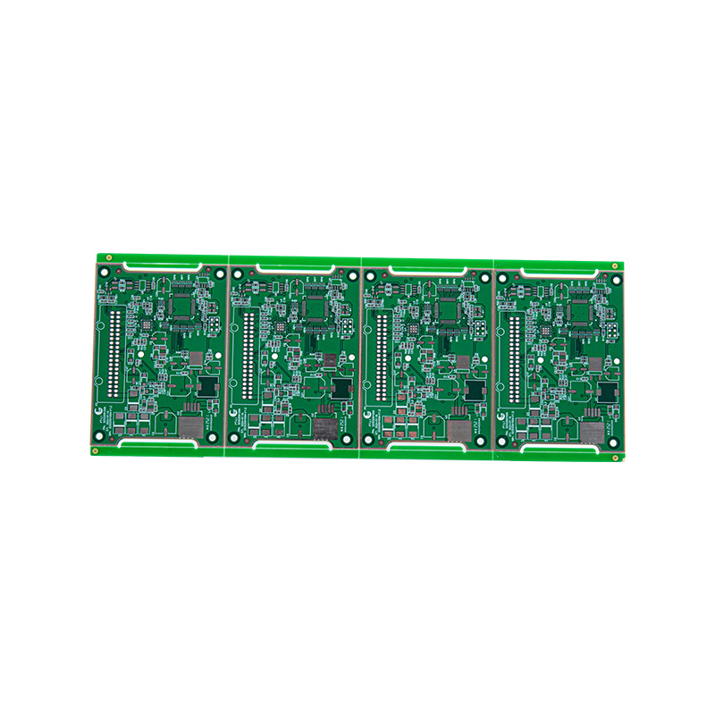
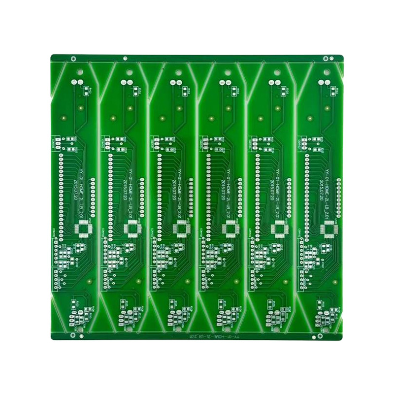
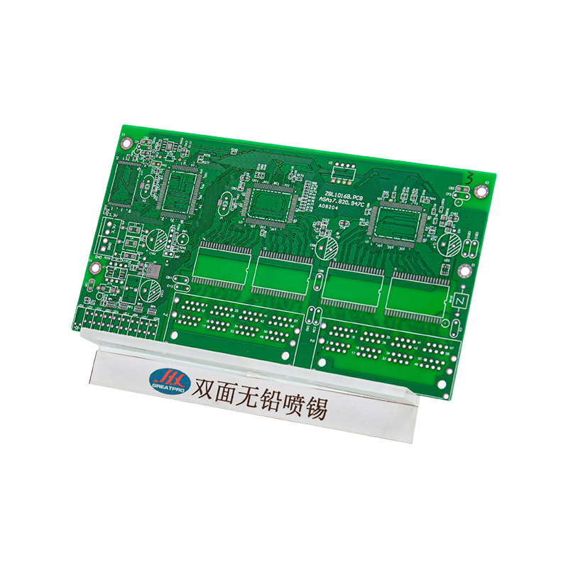
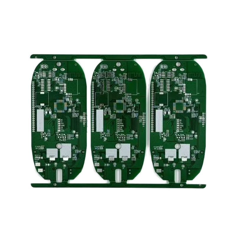
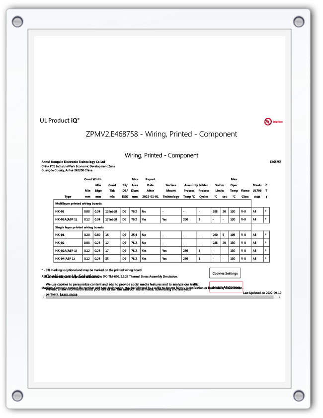
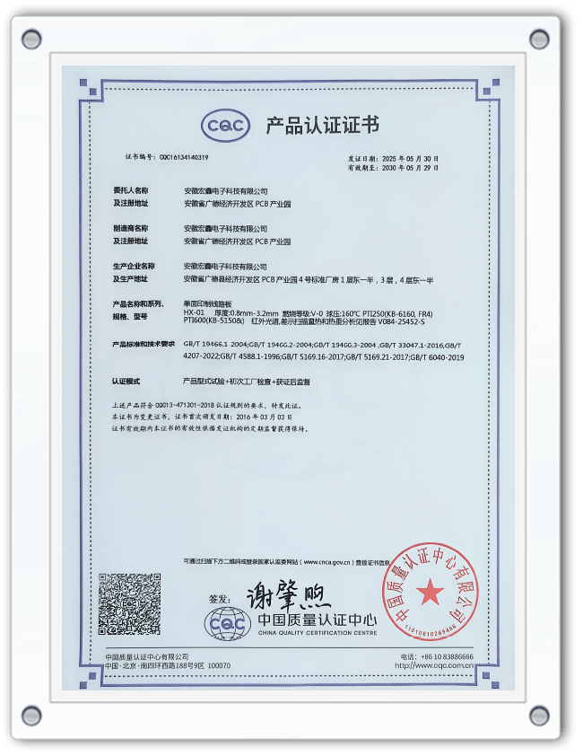
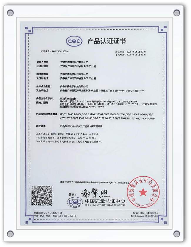
Double-Sided Lead-Free Soldered Green PCB With Enhanced Oxidation Resistance
Double-sided green lead-free soldered board, with its outstanding process adaptability, has become the cornerstone of high-reliability electronic design. The protective layer formed by the lead-free soldering layer is thicker and has a denser structure. Even after multiple reflow soldering or long-term storage, it can still maintain strong welding vitality and effectively resist oxidation erosion. This process endows the board with excellent mechanical stress resistance and stable power current-carrying performance, ensuring the product's persistent connection under vibration, shock or high current conditions. It is a solid guarantee for durable electronic products such as new energy control units, industrial power drives, automotive electronics and high-power power supply equipment.
- Specification
- About Hongxin
- Contact Us
|
Material |
FR-4, aluminium-based, ceramic, metal, copper-based, high-frequency, rigid-flex combined, halogen-free |
|
Board thickness |
0.3 - 6mm |
|
Copper thickness |
0.5oz - 5oz |
|
Number of layers |
1 - 32 layers |
|
Origin |
Anhui, China |
|
Surface treatment |
Ordinary tin plating, lead-free tin plating, OSP, nickel/gold plating, blue tape, silver plating, tin plating |
|
Minimum hole diameter |
0.25mm |
|
Minimum line width |
3mil (0.075mm) |
|
Minimum line spacing |
0.075mm |
|
Thickness-to-diameter ratio of holes |
10:19 |


 English
  Español
  Français
