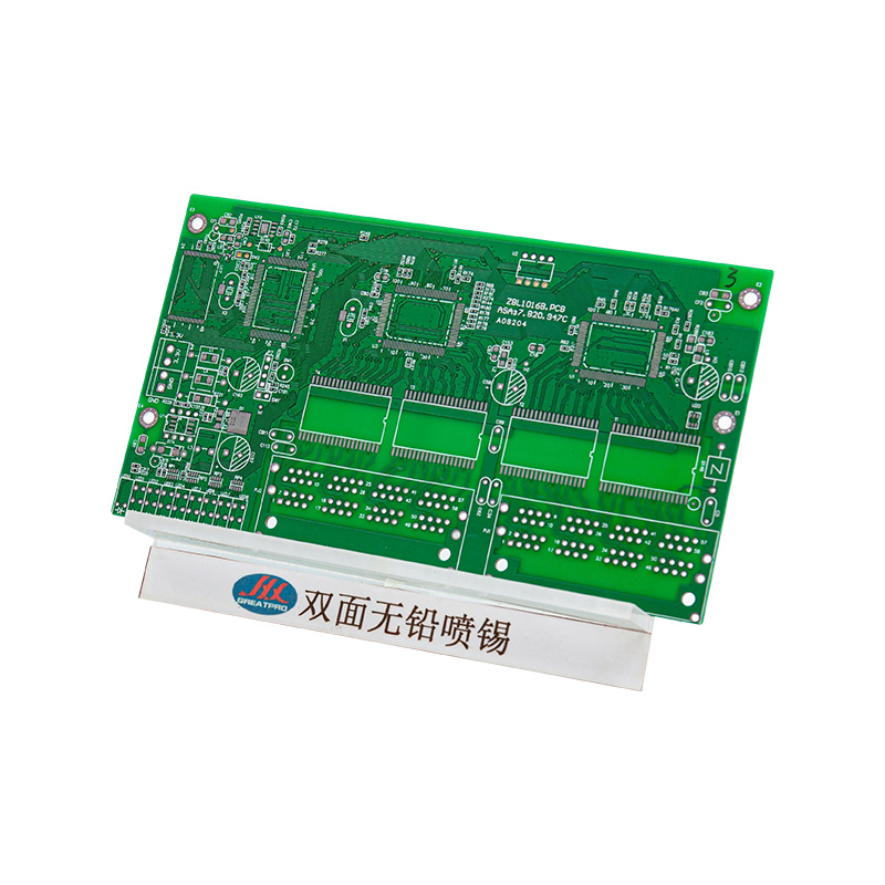
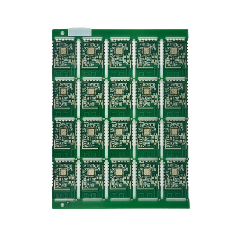
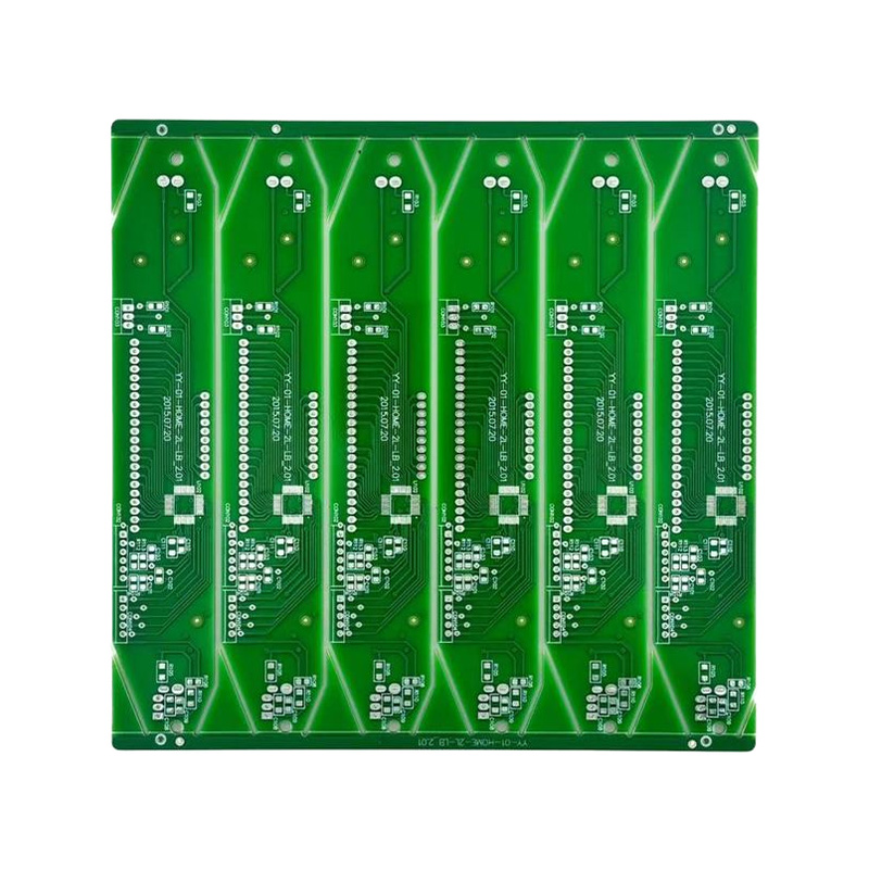
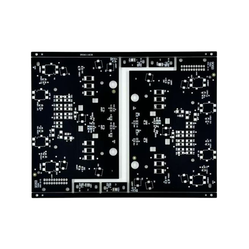
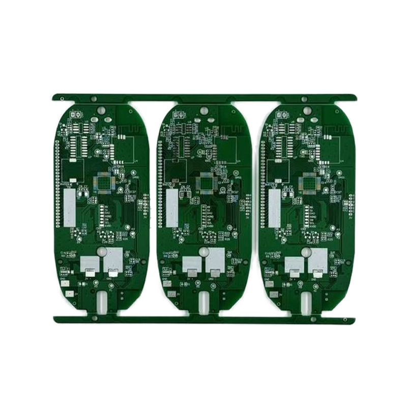
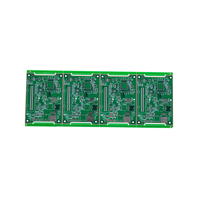
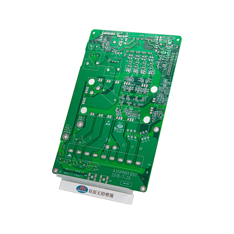
Double-Sided Green Lead-Free Tin-Plated Board
The double-sided green lead-free soldered PCB board adopts an environmentally friendly lead-free soldering surface process. The surface thickness of the pads is sufficient and durable, providing excellent solderability and strong welding strength, effectively ensuring the reliability of long-term connection of the products. The green solder mask layer has high visibility and excellent insulation protection performance. This product demonstrates outstanding cost-effectiveness and mature process, and is widely used in industrial control power supplies, automotive electronics, consumer electronic products, and smart home appliance controllers, which all have high requirements for durability.
- Specification
- About Hongxin
- Contact Us
|
Material |
FR-4, aluminium-based, ceramic, metal, copper-based, high-frequency, rigid-flex combined, halogen-free |
|
Board thickness |
0.3 - 6mm |
|
Copper thickness |
0.5oz - 5oz |
|
Number of layers |
1 - 32 layers |
|
Origin |
Anhui, China |
|
Surface treatment |
Ordinary tin plating, lead-free tin plating, OSP, nickel/gold plating, blue tape, silver plating, tin plating |
|
Minimum hole diameter |
0.25mm |
|
Minimum line width |
3mil (0.075mm) |
|
Minimum line spacing |
0.075mm |
|
Thickness-to-diameter ratio of holes |
10:12 |


 English
  Español
  Français

