


 English
 Español
 Français

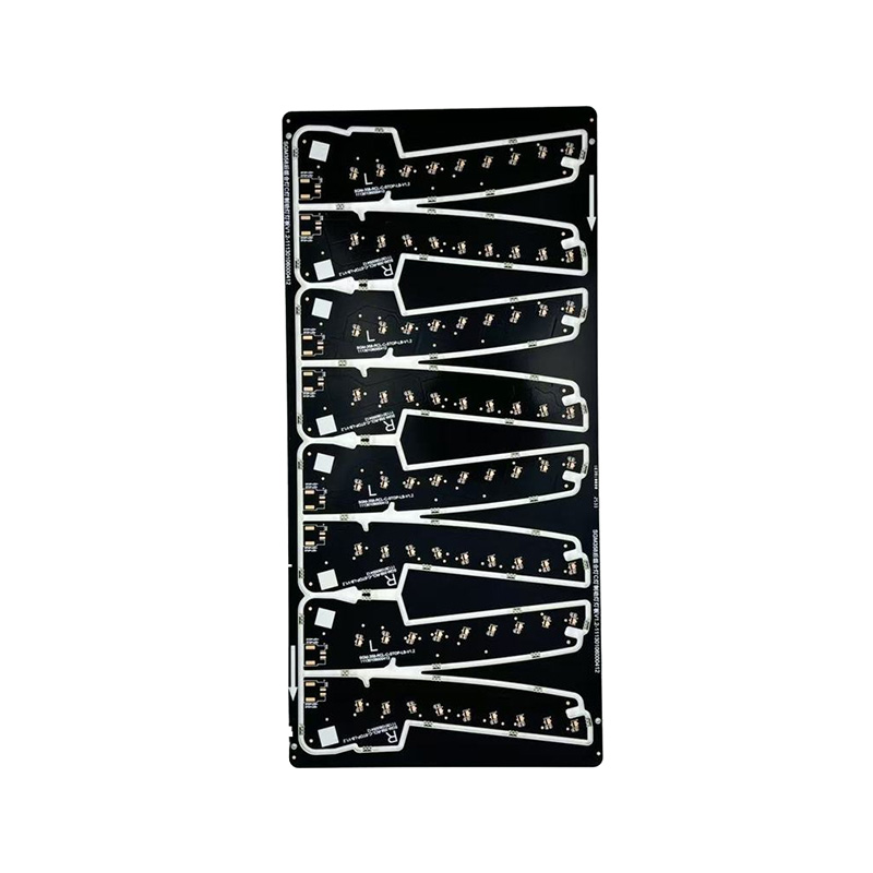

Double-Sided Black Lead-Free Solder Board
Double-sided black OSP PCB board, using the anti-oxidation (OSP) surface treatment process, forms a smooth and uniform protective film on the copper pads, featuring excellent solderability and good coplanarity. It is particularly suitable for precise welding of fine-pitch components. The black solder mask layer not only gives the product a unique visual sophistication but also effectively conceals the circuitry. It is an ideal choice for consumer electronics, smart home, industrial control, and automotive electronics, among others.
- Specification
- About Hongxin
- Contact Us
|
Material |
FR-4, aluminium-based, ceramic, metal, copper-based, high-frequency, rigid-flex combined, halogen-free |
|
Board thickness |
0.3 - 6mm |
|
Copper thickness |
0.5oz - 5oz |
|
Number of layers |
1 - 32 layers |
|
Origin |
Anhui, China |
|
Surface treatment |
Ordinary tin plating, lead-free tin plating, OSP, nickel/gold plating, blue tape, silver plating, tin plating |
|
Minimum hole diameter |
0.25mm |
|
Minimum line width |
3mil (0.075mm) |
|
Minimum line spacing |
0.075mm |
|
Thickness-to-diameter ratio of holes |
10:11 |
Product Overview
A double-sided black lead-free solder board is a two-layer PCB with a black LPI solder mask and a lead-free HASL (Hot Air Solder Leveling) surface finish. The lead-free tin coating provides solderable pads suitable for general SMT and through-hole assembly while complying with lead-free (RoHS) requirements. The black solder mask is selected for specific appearance or application needs. Board thickness, copper weight, and finish requirements should be confirmed against the customer's design files and engineering review.
Typical Applications
- Industrial control circuits
- Consumer electronics control boards
- Power and indicator circuits
- Automotive non-safety auxiliary modules
- General electronic assemblies requiring lead-free soldering
Key Features
- Lead-free HASL surface finish supports RoHS-compliant assembly processes
- Good solderability for both SMT and through-hole components
- Black solder mask for specific appearance requirements
- Cost-effective surface finish suitable for mass production
- Board thickness and copper weight customizable per design files
FAQ
Q: What is the difference between lead-free HASL and ENIG?
A: Lead-free HASL provides a solderable tin coating at lower cost, while ENIG offers a flatter pad surface with better oxidation resistance. The choice depends on pad pitch, storage period and assembly requirements.
Anhui Hongxin Electronic Technology Co., Ltd. is located in the China PCB Industrial Park, Guangde Economic Development District, Anhui Province. Established in October 2013, our factory occupies 20,000 square meters and employs 110 staff members, including over 7 professional engineers with more than 15 years of experience. The company's PCB products include 1-32 layer boards, high-Tg boards, thick copper boards, rigid-flex boards, high-frequency boards, hybrid dielectric laminated boards, buried via boards, metal-based boards, and halogen-free boards. High-precision PCB rapid prototyping is available, with bulk orders for single- and double-sided boards delivered within 6-7 days, 4-8 layer boards within 9-20 days, 10-16 layer boards within 20-25 days, 16-32 layer boards within 25-45 days, HDI boards within 25 days, and double-sided prototyping deliverable as quickly as 24 hours. We are committed to providing high-quality products and professional services to global customers, and we have the capability to deliver both large quantities and small batches. The surface treatment processes of our products are complete. The base material types include FR-1, 22F, CEM-1, CEM-3, FR-4 (with high Tg, halogen-free, etc.), high-frequency boards, and metal substrates. All product types have passed ISO9001, ISO14001, ISO45001, IATF16949 international quality management system certifications, as well as UL safety certifications. Our sales network extends from inland areas to Southeast Asia, Europe, and America. In the fierce market competition, we have always received high praise from customers.
Recommended Products


About
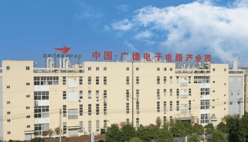
Anhui Hongxin Electronic Technology Co., Ltd.
Anhui Hongxin Electronic Technology Co., Ltd. is China Double-Sided Black Lead-Free Solder Board Suppliers and Wholesale Double-Sided Black Lead-Free Solder Board Factory. It is located in China P C B Industrial Park, Guangde Economic Development District, Anhui Province. Established in October 2 0 1 3, our factory occupied 8, 413 square meters and employs 110 staff members, including over 7 professional engineers with more than 15 years of experience. The company's P C B products include 1- 32 layer boards, high Tg boards, thick copper boards, rigid-flex boards, high- frequency boards, hybrid dielectric laminated boards, buried via boards, metal-based boards, and halogen- free boards. High-precision P C B rapid prototyping is available, with bulk orders for single and double -sided boards delivered within 6 - 7 days, 4 - 8 layer boards within 9 - 20 days, 10 - 16 layer boards within 20 - 25 days, 16 - 32 layer boards within 25 - 45 days, H D I boards within 25 days, and double- sided prototyping deliverable as quickly as 24 hours.
We are committed to providing high-quality products and professional services to global customers, and we have the capability to deliver orders of both large quantities and small batches. The surface treatment processes of our products are complete. The base material types include FR-1, 22F, CEM-1, CEM-3, FR-4 (with high Tg, halogen-free, etc.), high-frequency boards, and metal substrates. All product types have passed ISO9001, ISO14001, ISO45001, IATF16949 international quality management system certifications and UL safety certifications. Our sales network extends from inland areas to Southeast Asia and Europe and America. In the fierce market competition, we have always received high praise from customers.
Certificate Of Honour


 LET'S CREATE THE FUTURE TOGETHER

Contact Us Anytime
Copyright © Anhui Hongxin Electronic Technology Co., Ltd. All Rights
Reserved.
privacy
Wholesale Double-Sided Black Lead-Free Solder Board Suppliers, Factory

Message
We are committed to providing high-quality products and professional services to global customers
