


 English
  Español
  Français
6 Layer PCB Stackup, Quick Turn Fab, Solder Mask & Troubleshooting
When you need a reliable 6 layer pcb stackup example combined with quick turn pcb fab services, your design must balance symmetry, controlled impedance, and a robust solder mask on pcb application. If a prototype fails, knowing how to troubleshoot pcb problems quickly—starting with visual inspection of the solder mask and measuring plane-to-plane shorts—will save hours of debug time. This article delivers a field-proven stackup, a guide to selecting a fabrication partner, and a step-by-step fault-finding methodology.
Content
A Practical 6 Layer PCB Stackup Example for High-Density Designs
A well-designed 6 layer pcb stackup example provides two dedicated internal planes for power and ground, four signal layers, and excellent electromagnetic compatibility. The following stackup is suitable for digital and mixed-signal boards with fast rise times, and it is widely accepted by most quick turn pcb fab houses.
| Layer | Material | Thickness | Function |
|---|---|---|---|
| Top Layer | Copper (1 oz) | 1.4 mil | High-speed signal, components, solder mask |
| Dielectric 1 | Prepreg (FR-4) | 7 mil | Controlled impedance spacer |
| Layer 2 | Copper (0.5 oz) | 0.7 mil | Ground plane, continuous reference |
| Dielectric 2 | Core (FR-4) | 40 mil | Mechanical rigidity, isolation |
| Layer 3 | Copper (0.5 oz) | 0.7 mil | Signal (low-speed, parallel buses) |
| Layer 4 | Copper (0.5 oz) | 0.7 mil | Signal (low-speed, parallel buses) |
| Dielectric 3 | Core (FR-4) | 40 mil | Mechanical rigidity, isolation |
| Layer 5 | Copper (0.5 oz) | 0.7 mil | Power plane (split if necessary) |
| Dielectric 4 | Prepreg (FR-4) | 7 mil | Controlled impedance spacer |
| Bottom Layer | Copper (1 oz) | 1.4 mil | High-speed signal, components, solder mask |
This 6 layer pcb stackup example sandwiches a thick core between Layer 2-3 and Layer 4-5 to achieve a total thickness of roughly 62 mil (1.57 mm). The symmetry prevents warping during reflow, and the continuous ground plane on Layer 2 provides a tight return path for signals on the top layer. When ordering quick turn pcb fab, always specify controlled impedance on the outer layers and confirm that the fabricator can achieve the required dielectric thickness.
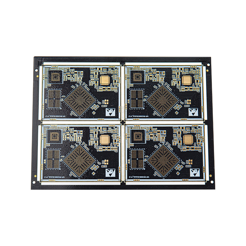
Leveraging Quick Turn PCB Fab Without Sacrificing Quality
Quick turn pcb fab services now deliver prototypes in 24 to 72 hours, but the rush must not compromise on the basics. A reliable quick-turn vendor should offer a minimum annular ring of 5 mil, a trace width and space of 4/4 mil, and a clear solder mask on pcb process with a registration accuracy of ±2 mil. Before releasing the Gerber files, verify that your design follows the fabricator's design rules and that every through-hole via has an adequate solder mask expansion.
A well-planned quick turn pcb fab order also includes electrical testing. Flying probe or fixture-based testing catches opens and shorts before the boards ship. Even the simplest 6 layer pcb stackup example can suffer from a via that did not plate correctly; catching this at the fab prevents hours of fruitless rework later. When you receive the boards, inspect the solder mask on pcb under magnification. A smeared or misaligned mask that encroaches on SMD pads will cause tombstoning and poor solder joints.
Solder Mask on PCB: More Than Just a Green Coating
The solder mask on pcb is a permanent polymer layer that insulates copper traces, prevents solder bridges, and protects against oxidation and mechanical damage. A properly applied liquid photoimageable solder mask has a thickness of 0.8 to 1.2 mil over the traces and defines the exact pad geometry through laser-direct imaging. For fine-pitch components, the mask web between pads must be at least 3 mil wide to remain intact after development.
When defining the solder mask on pcb in your design files, use a solder mask expansion of 2 to 3 mil around each pad. This value accounts for the typical registration shift during fabrication and ensures that the mask does not spill onto the pad surface. For high-reliability boards, specify a clear definition of tented vias versus open vias in the solder mask layer. Tented vias are covered entirely by the mask, while open vias are left exposed for test points or optional fill.
How to Troubleshoot PCB Failures Methodically
Learning how to troubleshoot pcb assemblies effectively means following a sequence that eliminates common causes before diving into complex signal analysis. The steps below assume the board is a freshly assembled prototype, possibly built using quick turn pcb fab, and is not functioning as expected.
- Perform a thorough visual inspection under a stereo microscope. Look for solder bridges, insufficient solder, tombstoned components, and any cracks or blisters in the solder mask on pcb that might expose copper.
- Measure the resistance between each power rail and ground with a multimeter. A reading below 10 ohms often indicates a short. If the board uses a split plane as described in the 6 layer pcb stackup example, check each voltage domain individually.
- Power up the board with a current-limited supply set to 50 mA. If the current limits immediately, use a thermal camera or freeze spray to locate the overheated component. A shorted multilayer ceramic capacitor is a frequent culprit.
- With the board powered, verify all voltage regulators output the correct voltage. Ripple should be less than 2 percent of the DC value. Excessive ripple may point to a missing or damaged decoupling capacitor.
- Inject a known signal at the input and trace it through the signal chain with an oscilloscope. Compare the waveform against the expected values at each test point. A clean signal that disappears at a specific pin suggests a bad solder joint on that pad—often visible by probing the solder mask on pcb around the pin for discoloration.
A significant number of faults on a prototype board originate from manufacturing defects that could have been flagged by a more rigorous quick turn pcb fab quality check. Always re-verify the bare PCB before assembly by measuring trace continuity and checking for solder mask slivers that can bridge adjacent pads. By combining a robust 6 layer pcb stackup example, a reliable fabrication process, and systematic troubleshooting, you reduce prototype iterations and keep your project on schedule.
Recommended Products
-

6-Layer Gold-Plated Board, Line Width And Spacing Of 3/3, BGA, Half-Hole Technology
-
Double-Sided Green Lead-Free Soldered PCB For Power & Automotive Electronics
-
4 Layers Green OSP PCB
-
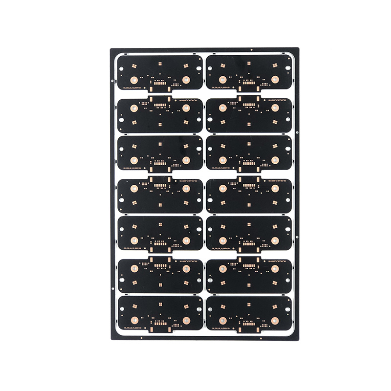
Double-Sided Black 0.3-6Mm OSP PCB Board
-
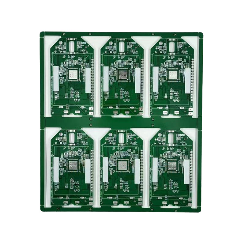
Double-Sided Lead-Free Soldered Green PCB With Enhanced Oxidation Resistance
-
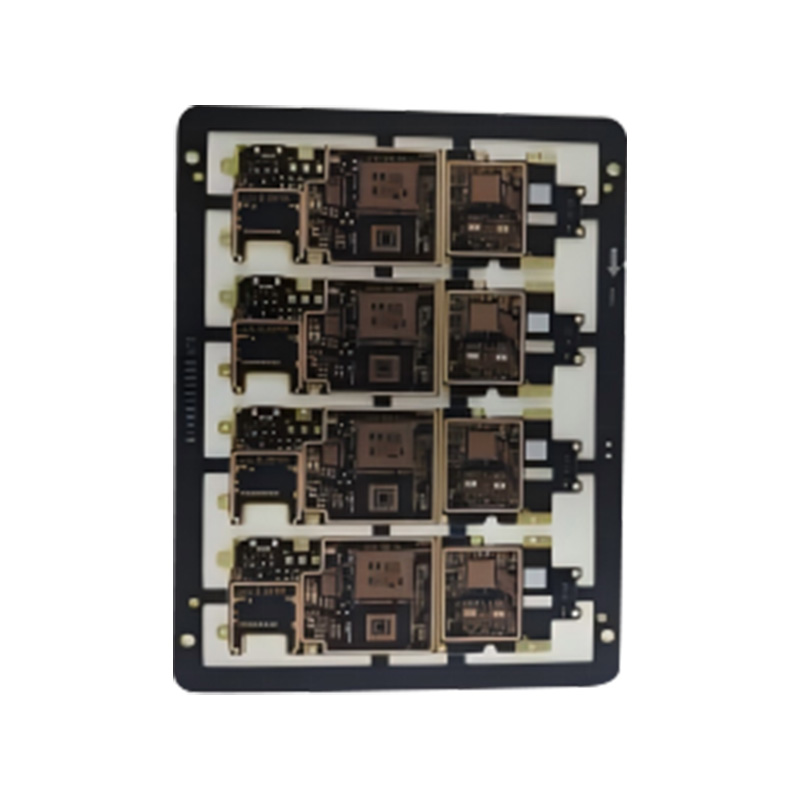
2-Layer 6-Level HDI Board
 LET'S CREATE THE FUTURE TOGETHER

Contact Us Anytime
Copyright © Anhui Hongxin Electronic Technology Co., Ltd. All Rights
Reserved.
privacy
Wholesale Printed Circuit Board Suppliers, Manufacturers

