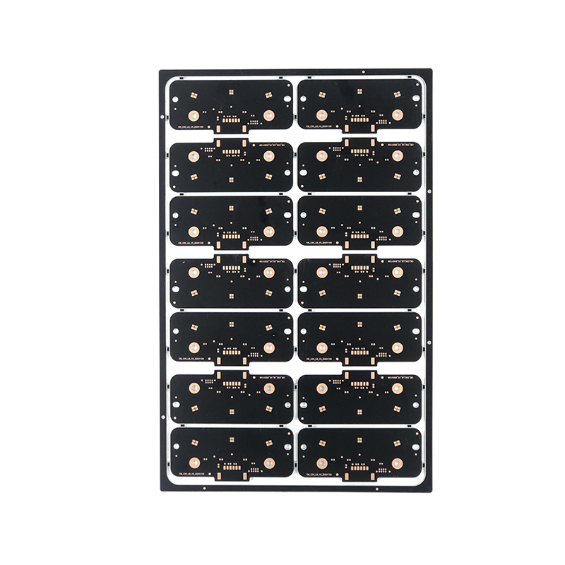
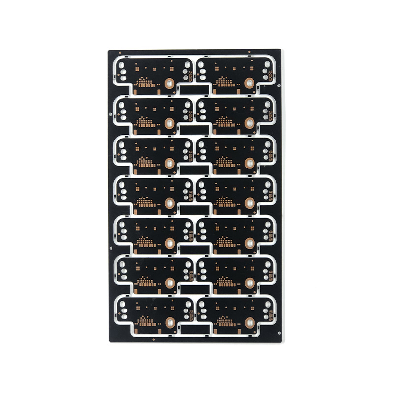
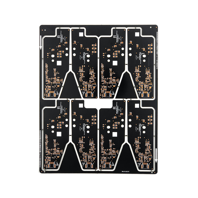
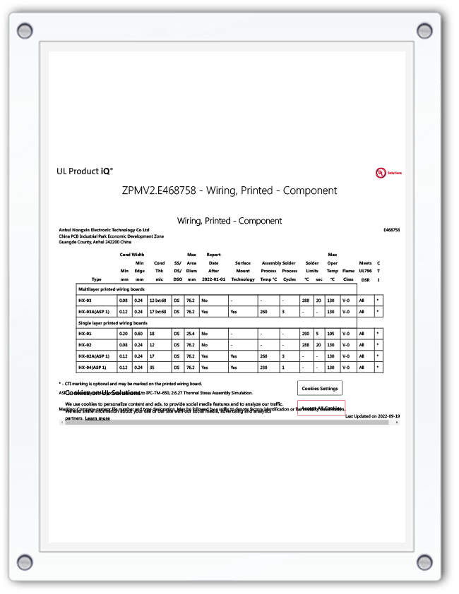
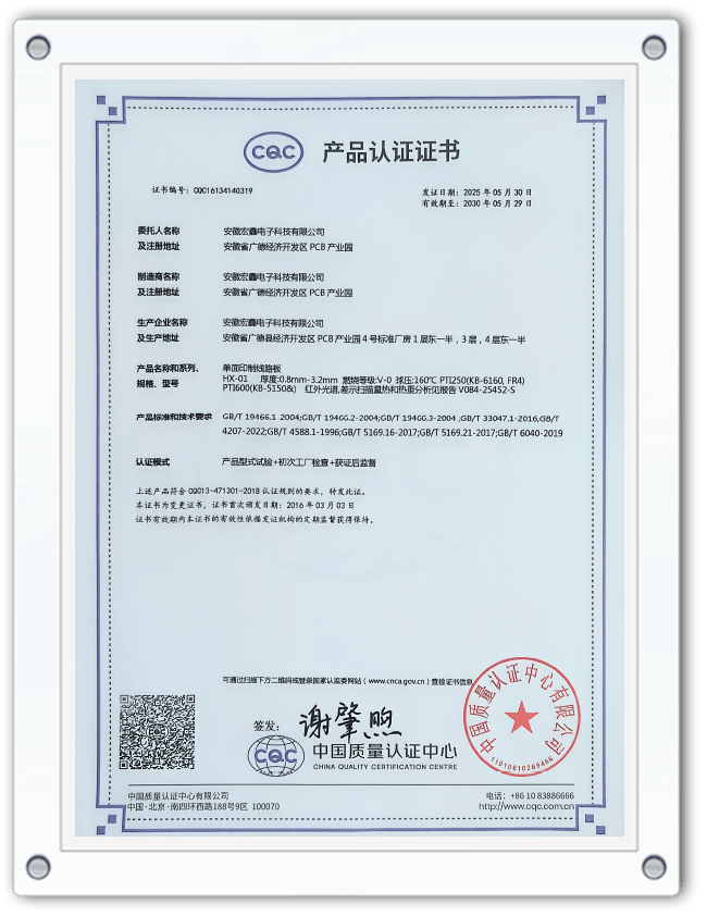
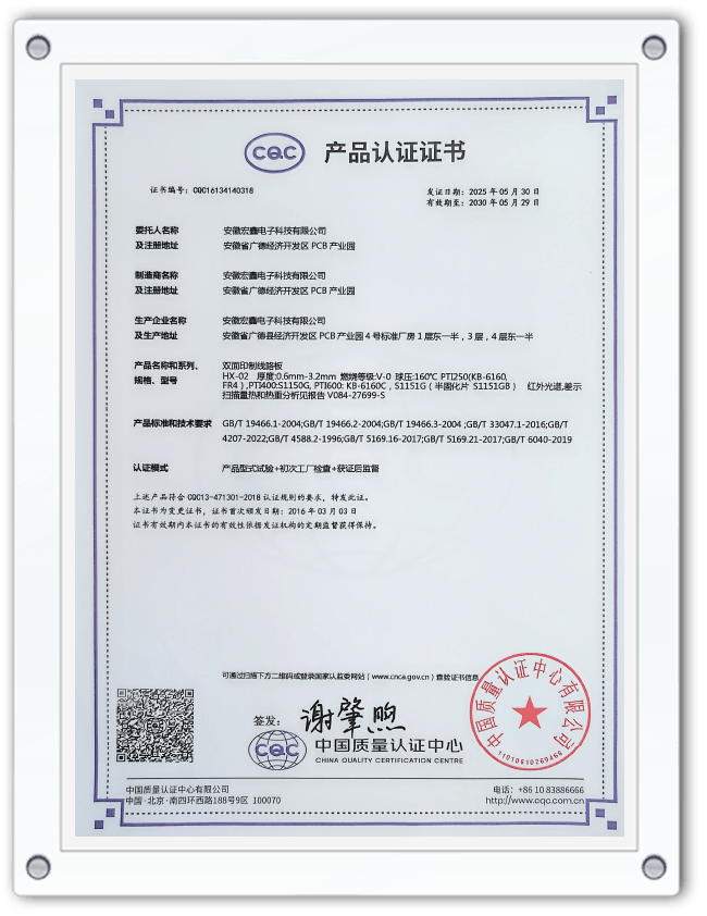
4 Layers Green OSP PCB
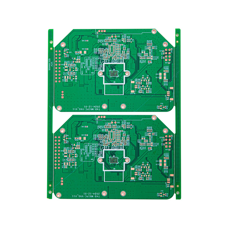
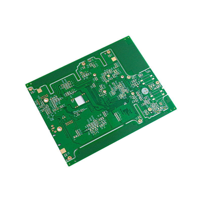
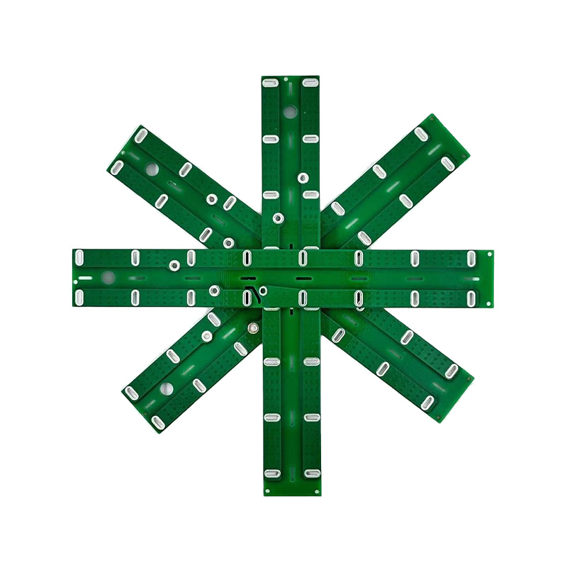
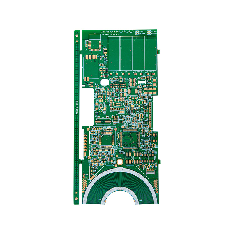
Four-layer double-sided green OSP boards, using high-Tg FR-4 substrate and environmentally friendly OSP (organic soldering flux) surface treatment process, the green solder mask layer complies with the production standard specifications of the PCB industry, can directly be adapted to the visual positioning system of the automated production line, improving the accuracy and efficiency of surface mount, insertion and AOI inspection, and significantly reducing the production line debugging cost. The OSP layer is formed by a precise coating process into a uniform and dense organic protective film, with excellent high-temperature soldering performance, effectively avoiding assembly defects such as false soldering and continuous tin, and without heavy metal residues. It is widely used in industrial automation control motherboards, consumer electronic power drive boards, core circuits of security monitoring equipment, automotive electronic auxiliary modules, etc., and is a cost-effective, high-performance and compliant mass production solution.
- Specification
- About Hongxin
- Contact Us
|
Material |
FR-4, aluminium-based, ceramic, metal, copper-based, high-frequency, rigid-flex combined, halogen-free |
|
Board thickness |
0.3 - 6mm |
|
Copper thickness |
0.5oz - 5oz |
|
Number of layers |
1 - 32 layers |
|
Origin |
Anhui, China |
|
Surface treatment |
Ordinary tin plating, lead-free tin plating, OSP, nickel/gold plating, blue tape, silver plating, tin plating |
|
Minimum hole diameter |
0.25mm |
|
Minimum line width |
3mil (0.075mm) |
|
Minimum line spacing |
0.075mm |
|
Ratio of board thickness to hole diameter |
10:5 |


 English
  Español
  Français
