Four-Layer Double-Sided Green OSP Board

Home / Products / PCB / Multilayer PCB / Four-Layer Double-Sided Green OSP Board

Four-Layer Double-Sided Green OSP Board

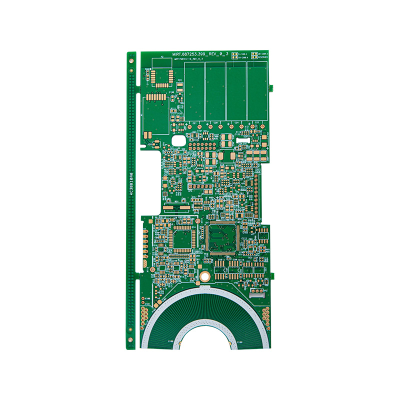
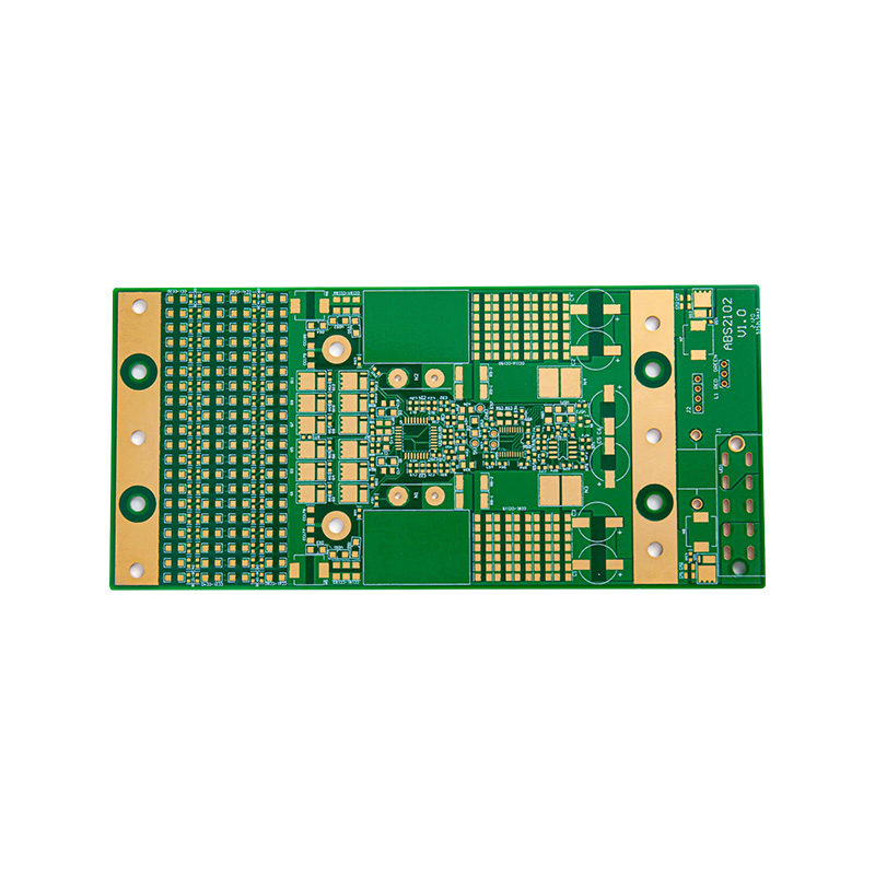
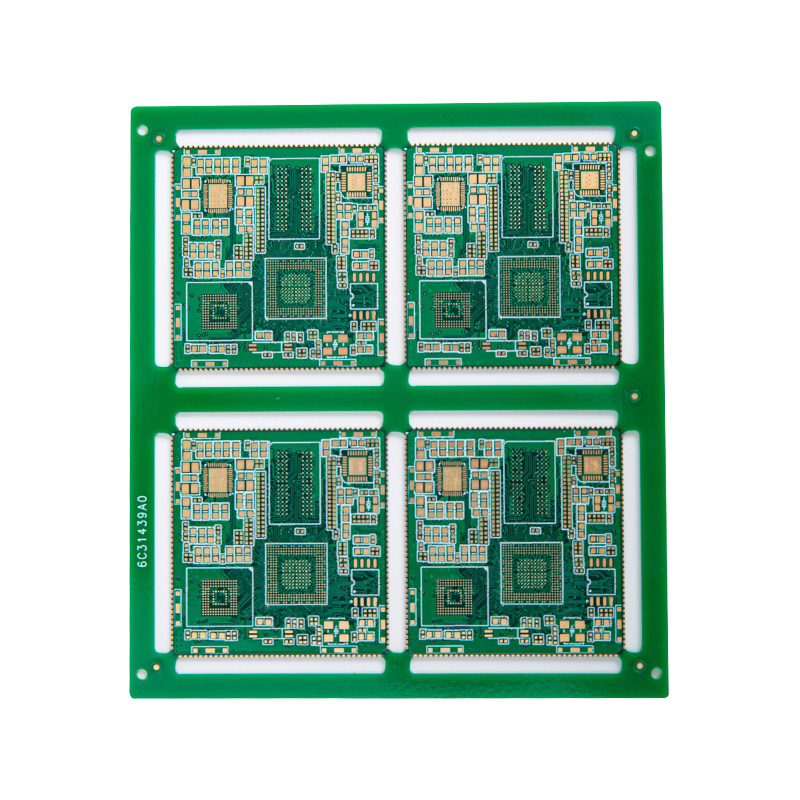
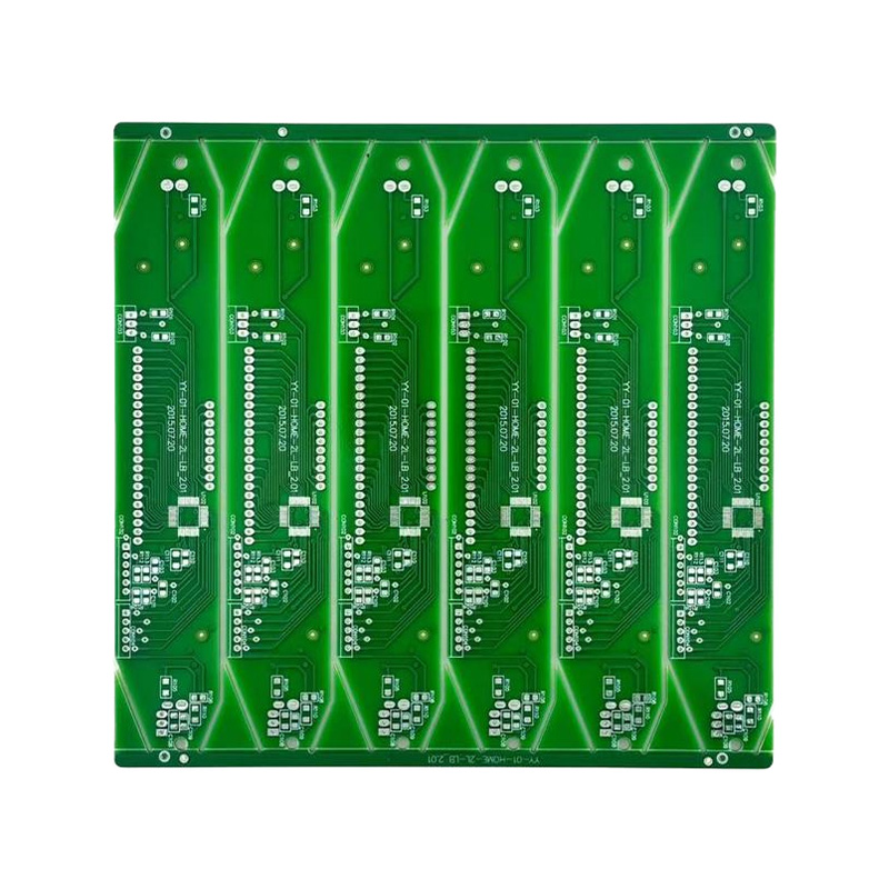
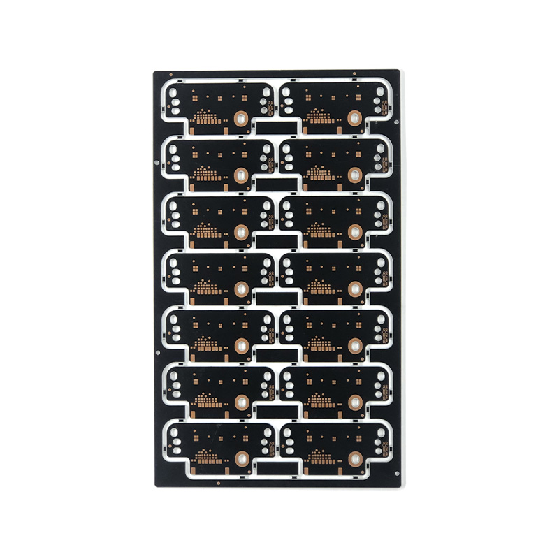
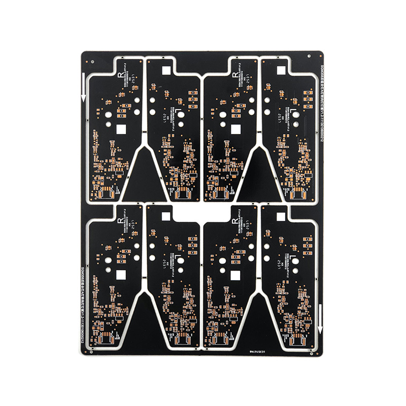
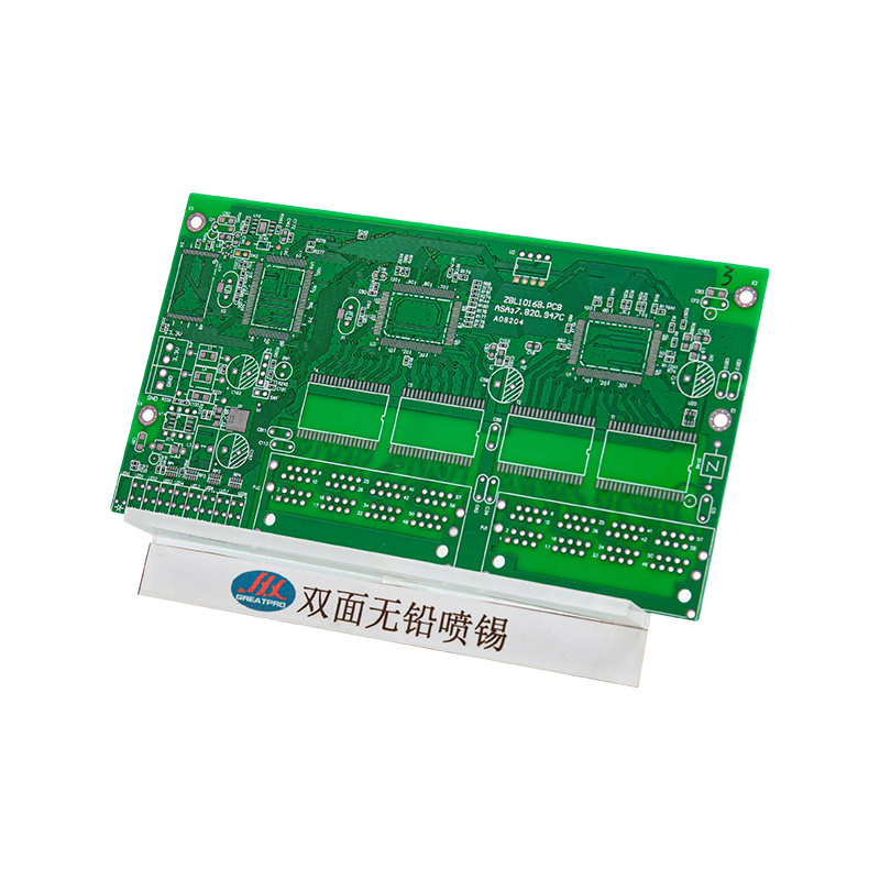
Four-layer double-sided green OSP boards, using high-reliability FR-4 base material and environmentally friendly OSP surface treatment, the green solder mask layer conforms to the visual standards of mass production in the PCB industry. It can seamlessly adapt to the automatic production line's soldering and inspection processes, significantly improving the production efficiency of batch production. The organic protective film formed by the OSP process has high temperature resistance and strong oxidation resistance, can precisely avoid the risk of welding short circuits, and with the four-layer optimized layering design, realizes efficient isolation of power and signal lines, effectively reducing signal crosstalk, and ensuring stable transmission of medium and high-speed circuits. The product supports flexible customization of board thickness, copper thickness, and fine line specifications, is compatible with various packaging processes, has undergone strict environmental reliability tests, and is suitable for mass production scenarios in industrial control, consumer electronics, security equipment, etc. It is a high-quality PCB solution that combines high cost performance, stable performance, and environmental compliance.

Contact Us
  • Specification
  • About Hongxin
  • Contact Us

Material

 FR-4, aluminium-based, ceramic, metal, copper-based, high-frequency, rigid-flex combined, halogen-free

Board thickness

 0.3 - 6mm

Copper thickness

 0.5oz - 5oz

Number of layers

 1 - 32 layers

Origin

 Anhui, China

Surface treatment

 Ordinary tin plating, lead-free tin plating, OSP, nickel/gold plating, blue tape, silver plating, tin plating

Minimum hole diameter

 0.25mm

Minimum line width

 3mil (0.075mm)

Minimum line spacing

 0.075mm

Ratio of board thickness to hole diameter

 10:6

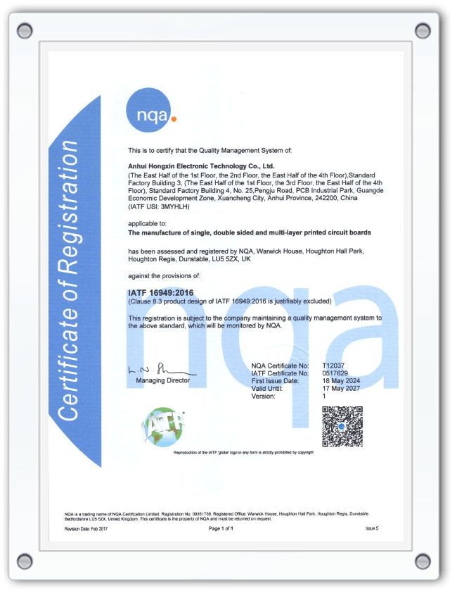
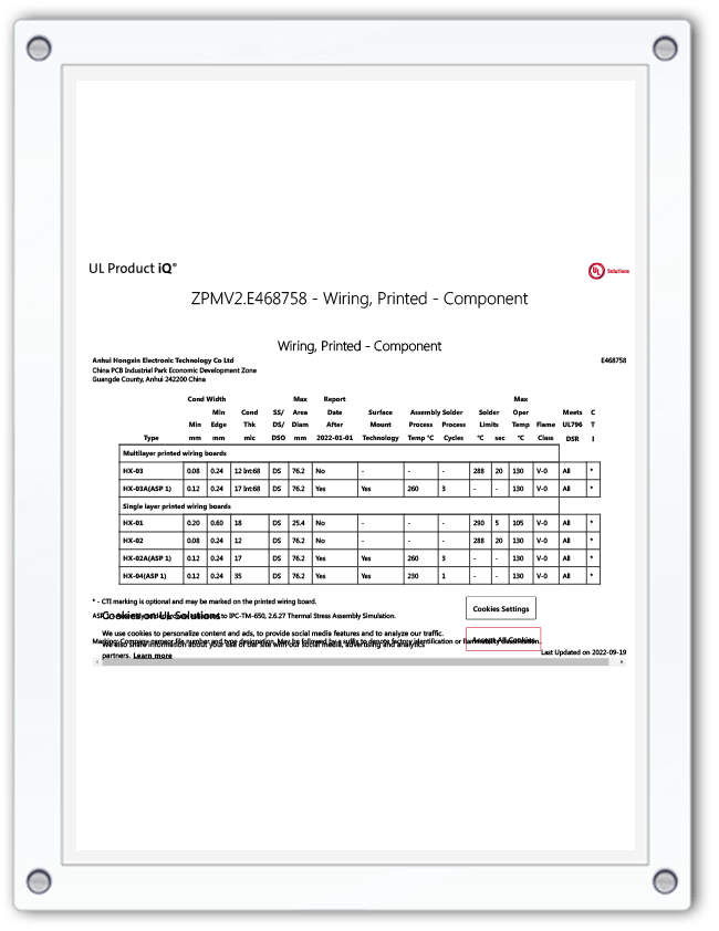
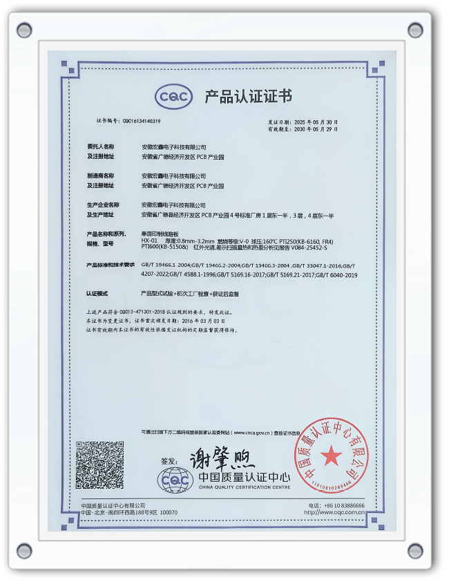
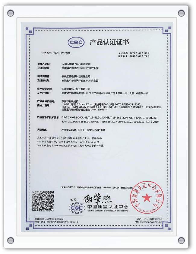
Anhui Hongxin Electronic Technology Co., Ltd. located in China P C B Industrial Park, Guangde Economic Development District, Anhui Province. Established in October 2 0 1 3, our factory occupied 2000 square meters and employs 158 staff members, including over 7 professional engineers with more than 15 years of experience. The company's P C B products include 1- 32 layer boards, high Tg boards, thick copper boards, rigid-flex boards, high- frequency boards, hybrid dielectric laminated boards, buried via boards, metal-based boards, and halogen- free boards. High-precision P C B rapid prototyping is available, with bulk orders for single and double -sided boards delivered within 6 - 7 days, 4 - 8 layer boards within 9 - 20 days, 10 - 16 layer boards within 20 - 25 days, 16 - 32 layer boards within 25 - 45 days, H D I boards within 25 days, and double- sided prototyping deliverable as quickly as 24 hours. We are committed to providing high-quality products and professional services to global customers, and we have the capability to deliver orders of both large quantities and small batches. The surface treatment processes of our products are complete. The base material types include FR-1, 22F, CEM-1, CEM-3, FR-4 (with high Tg, halogen-free, etc.), high-frequency boards, and metal substrates. All product types have passed ISO9001, ISO14001, ISO45001, IATF16949 international quality management system certifications and UL safety certifications. Our sales network extends from inland areas to Southeast Asia and Europe and America. In the fierce market competition, we have always received high praise from customers.
About
Anhui Hongxin Electronic Technology Co., Ltd.
Anhui Hongxin Electronic Technology Co., Ltd. located in China P C B Industrial Park, Guangde Economic Development District, Anhui Province. Established in October 2 0 1 3, our factory occupied 8, 413 square meters and employs 158 staff members, including over 7 professional engineers with more than 15 years of experience. The company's P C B products include 1- 32 layer boards, high Tg boards, thick copper boards, rigid-flex boards, high- frequency boards, hybrid dielectric laminated boards, buried via boards, metal-based boards, and halogen- free boards. High-precision P C B rapid prototyping is available, with bulk orders for single and double -sided boards delivered within 6 - 7 days, 4 - 8 layer boards within 9 - 20 days, 10 - 16 layer boards within 20 - 25 days, 16 - 32 layer boards within 25 - 45 days, H D I boards within 25 days, and double- sided prototyping deliverable as quickly as 24 hours. We are committed to providing high-quality products and professional services to global customers, and we have the capability to deliver orders of both large quantities and small batches. The surface treatment processes of our products are complete. The base material types include FR-1, 22F, CEM-1, CEM-3, FR-4 (with high Tg, halogen-free, etc.), high-frequency boards, and metal substrates. All product types have passed ISO9001, ISO14001, ISO45001, IATF16949 international quality management system certifications and UL safety certifications. Our sales network extends from inland areas to Southeast Asia and Europe and America. In the fierce market competition, we have always received high praise from customers.
News
Multilayer PCB Industry knowledge