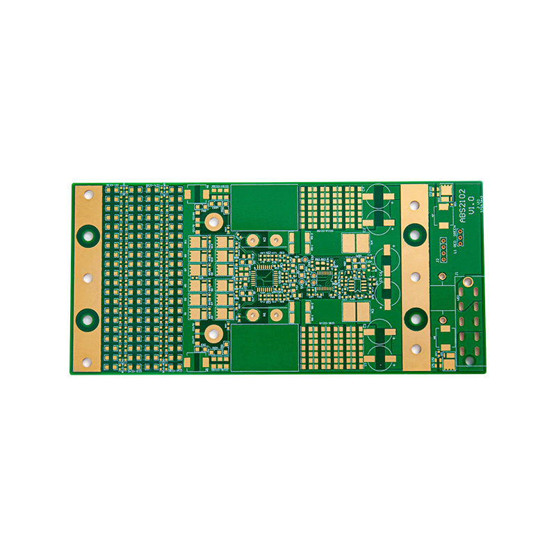
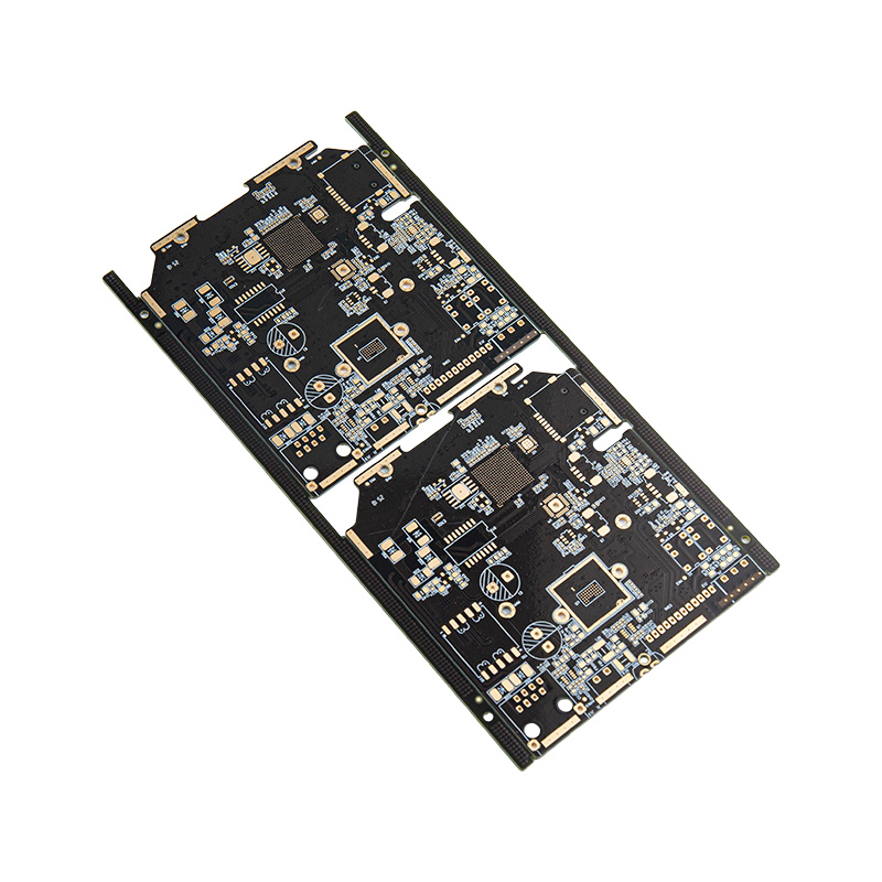
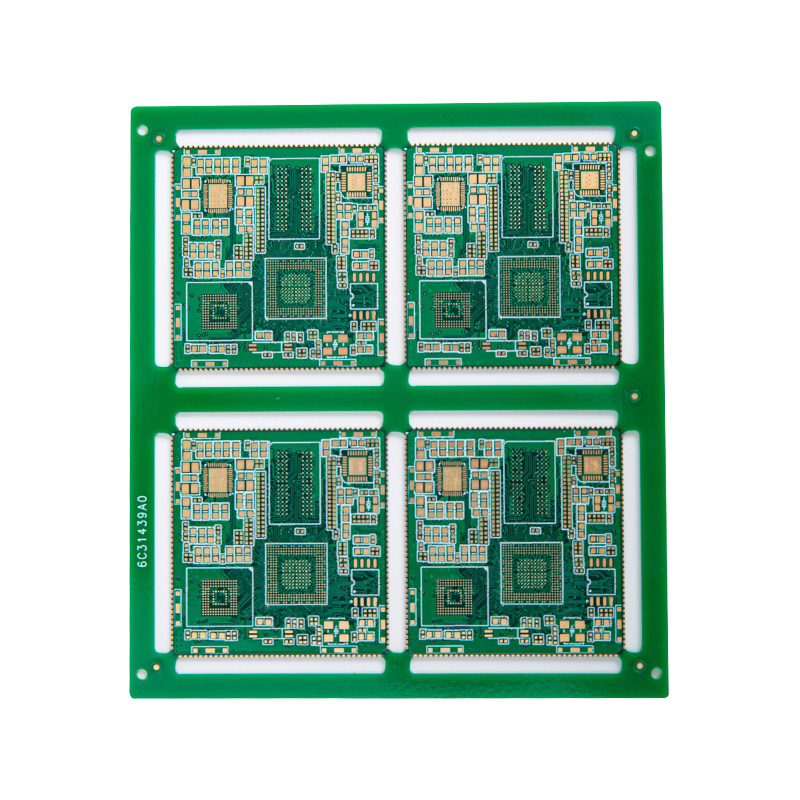
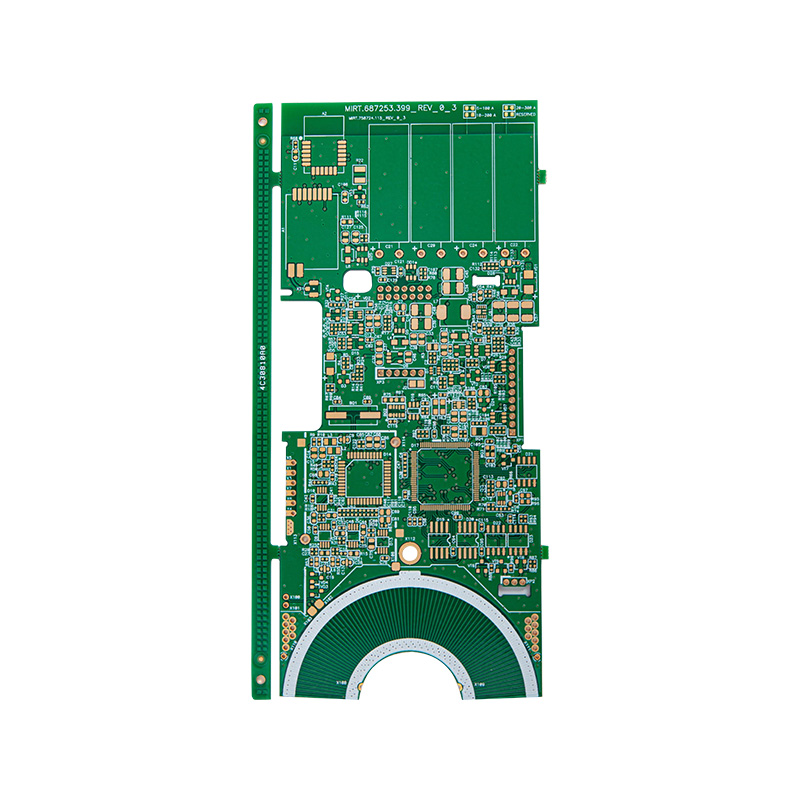
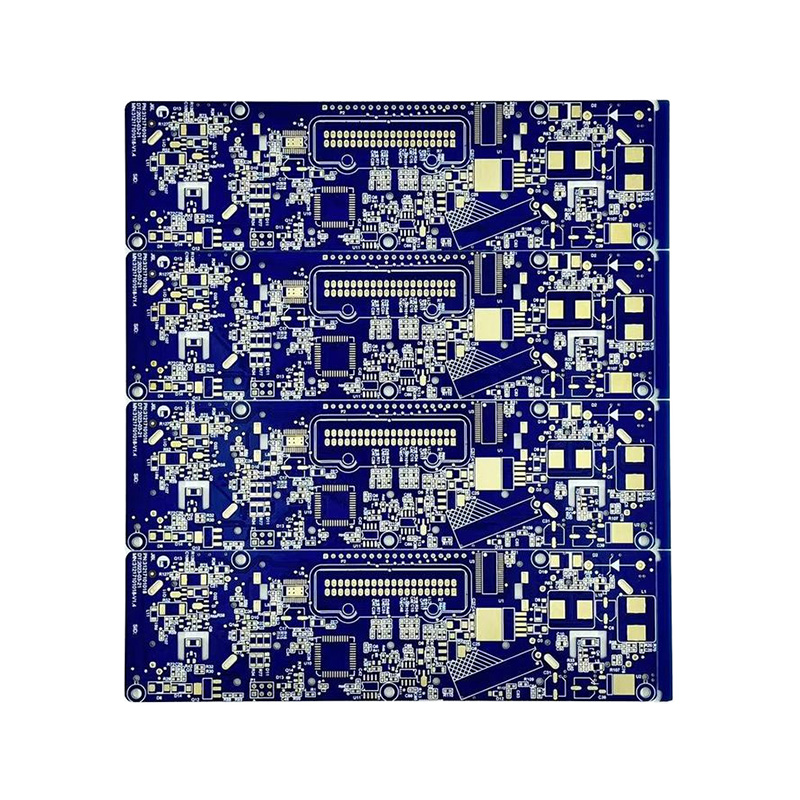
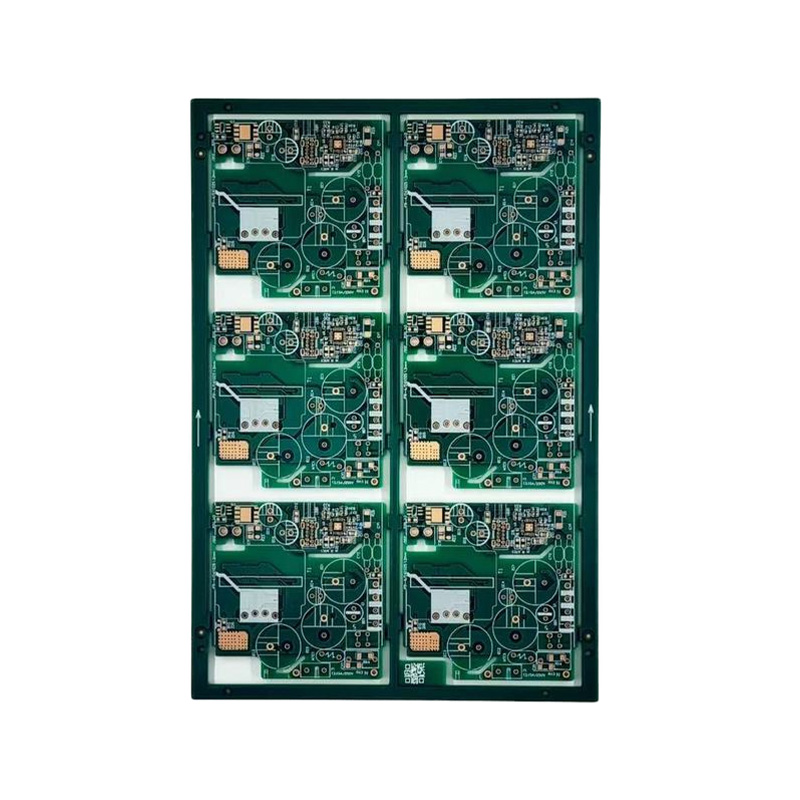
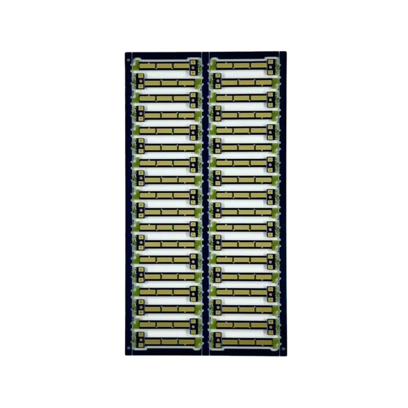
Four-Layer Double-Sided Greenized Gold Plate
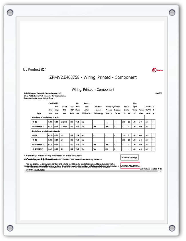
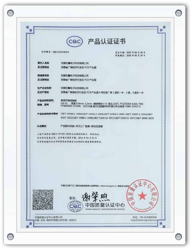
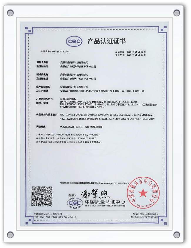
A four-layer double-sided greenized gold plate, using high-precision laminating technology and industry-standard bright green solder mask layer combined with gold plating treatment, realizes the separation design of signal layer and power layer in the four-layer circuit layout, effectively reducing electromagnetic interference. The surface layer of gold plating has an accurate thickness controlled within 0.1-0.2 μm, with low contact resistance and excellent wear resistance. The lead-free and halogen-free process fully complies with the H environmental standard. At the same time, the edge adopts CNC precision cutting technology, with no burrs after disassembly and high dimensional accuracy, suitable for batch assembly on automated production lines. It is applicable to industrial automation control motherboards, high-end automotive electronic modules, precision testing instrument circuits, 5G communication terminal equipment, etc., and is a high-performance PCB solution that takes into account the adaptability of complex circuits, environmental tolerance and environmental compliance.
- Specification
- About Hongxin
- Contact Us
|
Material |
FR-4, aluminium-based, ceramic, metal, copper-based, high-frequency, rigid-flex combined, halogen-free |
|
Board thickness |
0.3 - 6mm |
|
Copper thickness |
0.5oz - 5oz |
|
Number of layers |
1 - 32 layers |
|
Origin |
Anhui, China |
|
Surface treatment |
Ordinary tin plating, lead-free tin plating, OSP, nickel/gold plating, blue tape, silver plating, tin plating |
|
Minimum hole diameter |
0.25mm |
|
Minimum line width |
3mil (0.075mm) |
|
Minimum line spacing |
0.075mm |
|
Ratio of board thickness to hole diameter |
10:25 |


 English
  Español
  Français
