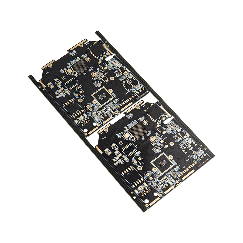
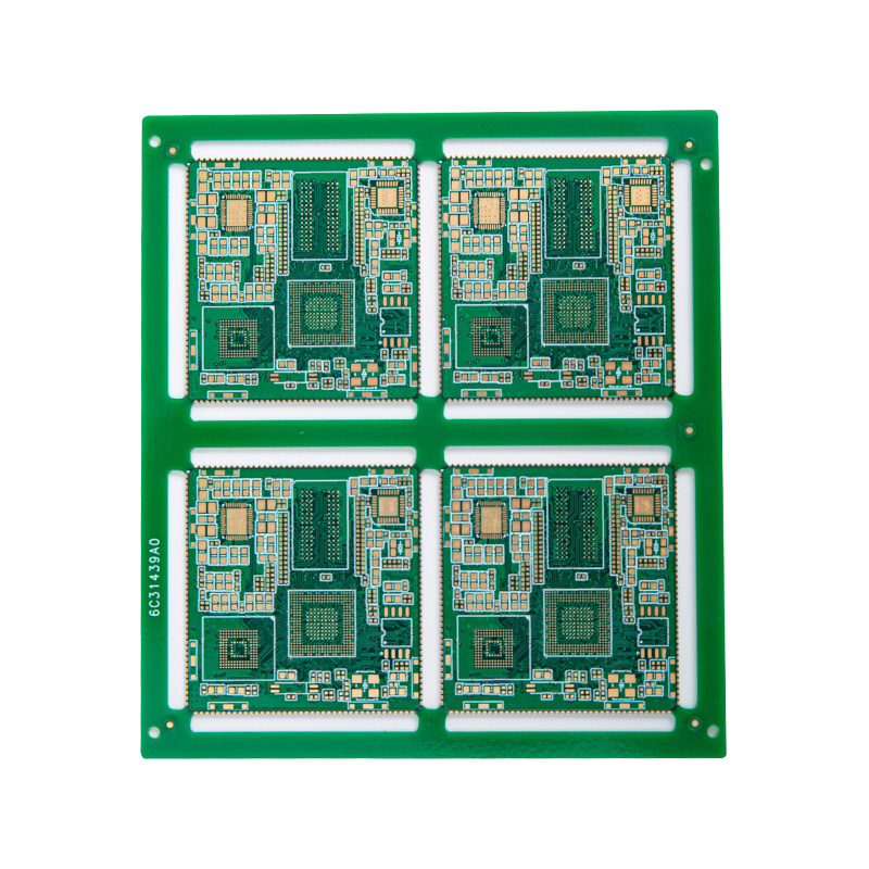
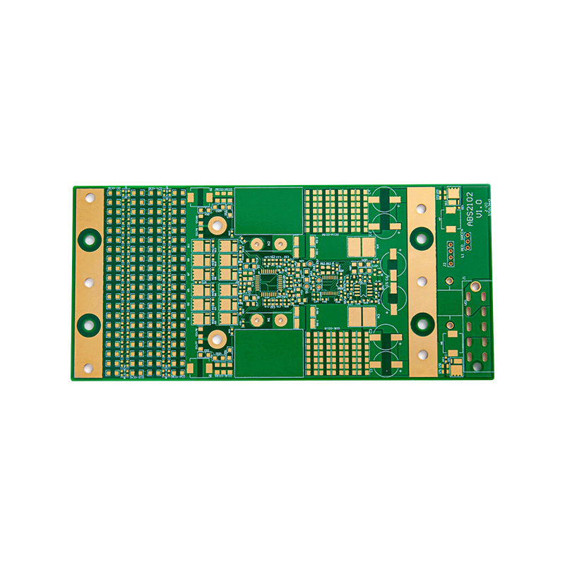
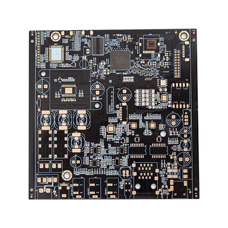
Four-Layer Double-Sided Blackened Gold Plate
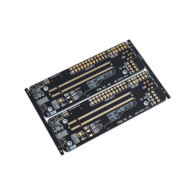
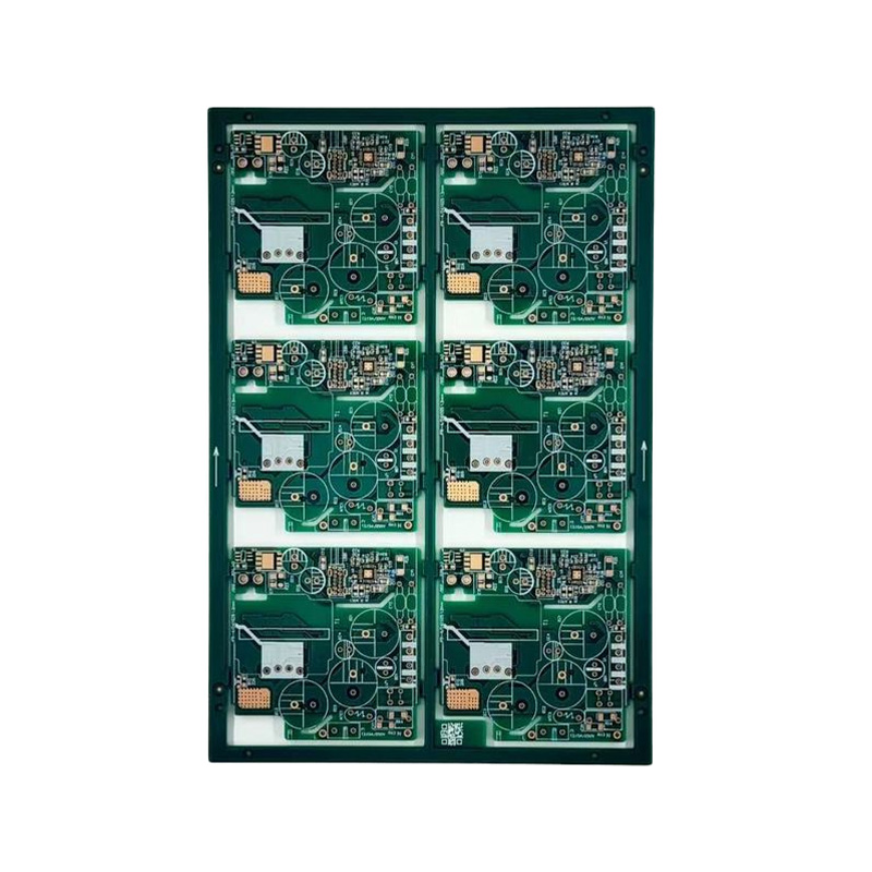
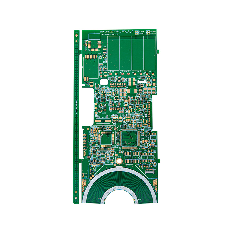
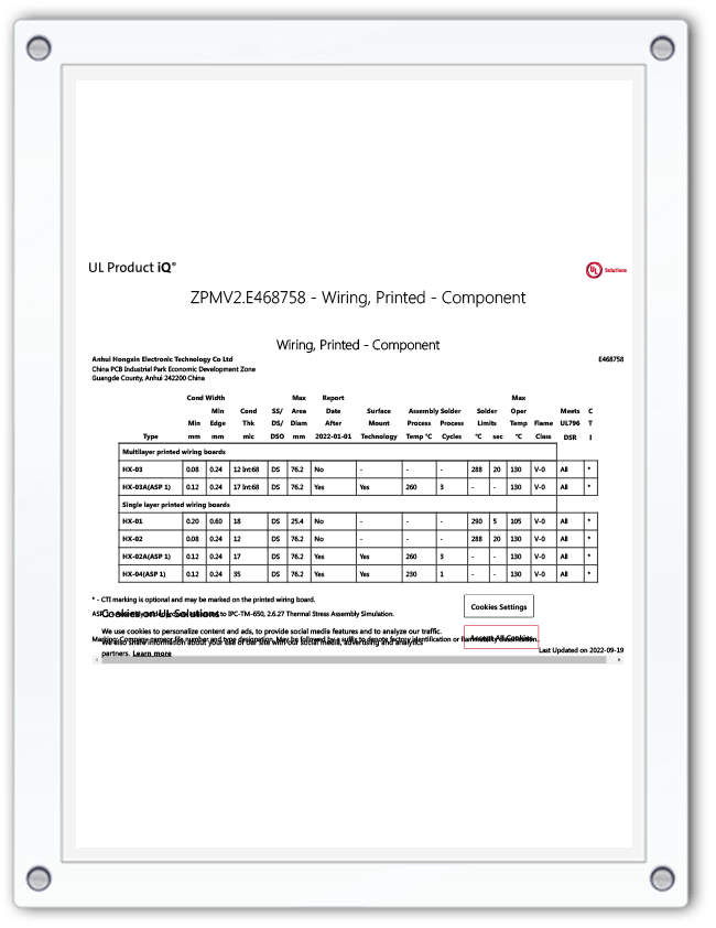
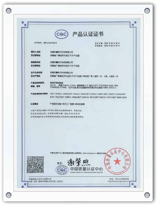
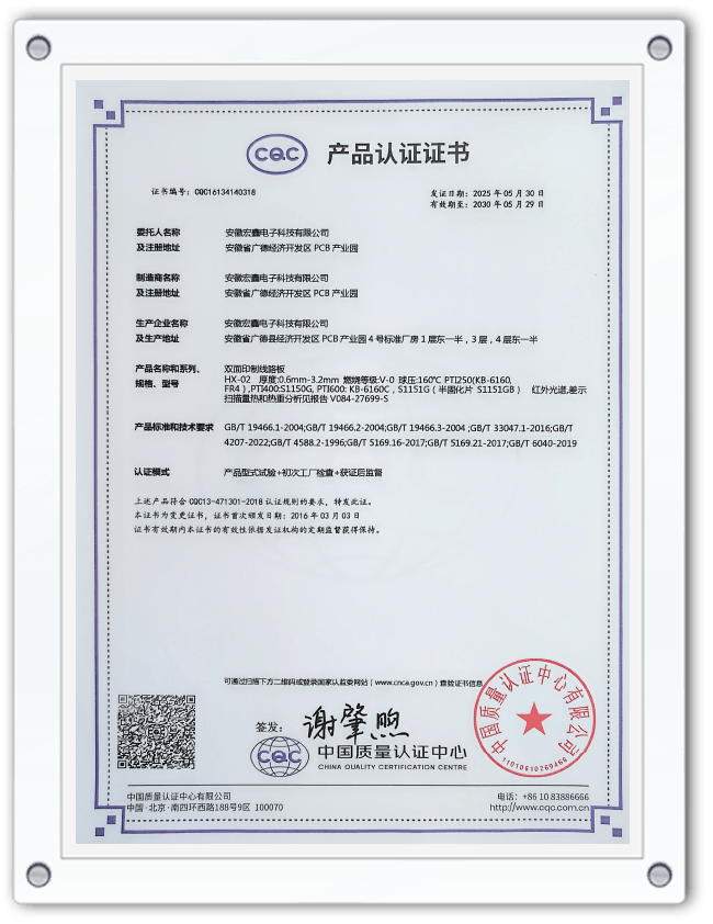
A four-layer double-sided blackened gold board, featuring a four-layer circuit structure and double-sided gold plating process. The black solder mask layer not only ensures a high-end appearance but also maintains the confidentiality of the circuitry. The surface of the gold plating is resistant to oxidation and wear, enhancing both conductivity and soldering stability, and is suitable for high-frequency usage scenarios. The four-layer layout supports complex circuit designs, and combined with precise impedance control, it can meet the requirements for medium and high-speed signal transmission. It can also be flexibly customized for board thickness, copper thickness, and line width and spacing, and is compatible with precision pads, half-holes, and other processes. Its core advantages are multi-layer expansion capability + durable gold plating + appearance confidentiality. It is mainly applied in industrial control modules, automotive electronic precision components, etc., and is a high-quality PCB solution that meets multiple dimensions of requirements.
- Specification
- About Hongxin
- Contact Us
|
Material |
FR-4, aluminium-based, ceramic, metal, copper-based, high-frequency, rigid-flex combined, halogen-free |
|
Board thickness |
0.3 - 6mm |
|
Copper thickness |
0.5oz - 5oz |
|
Number of layers |
1 - 32 layers |
|
Origin |
Anhui, China |
|
Surface treatment |
Ordinary tin plating, lead-free tin plating, OSP, nickel/gold plating, blue tape, silver plating, tin plating |
|
Minimum hole diameter |
0.25mm |
|
Minimum line width |
3mil (0.075mm) |
|
Minimum line spacing |
0.075mm |
|
Thickness-to-diameter ratio of holes |
10:1 |


 English
  Español
  Français
