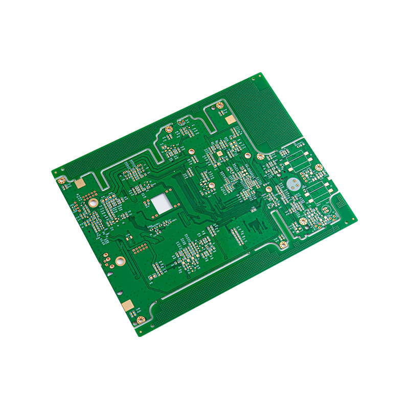
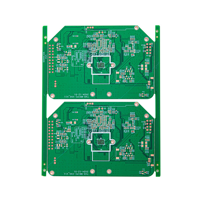
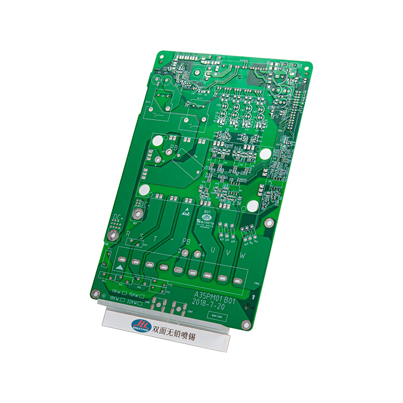
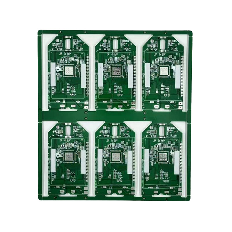
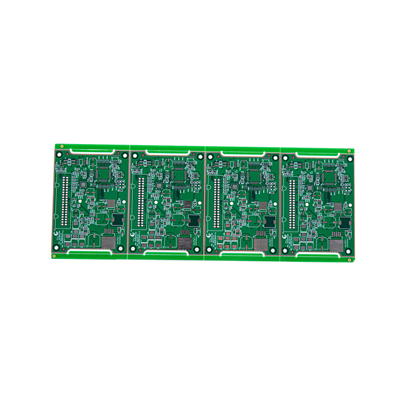
Green Fr-4 OEM Multilayer Gold Plating PCB
A four-layer double-sided greenized gold plate, using the industry-standard green solder mask layer combined with double-sided gold plating technology, presents a green appearance that aligns with the conventional identification habits in electronic manufacturing, facilitating efficient assembly and quality inspection on the production line. The double-sided gold plating surface features low contact resistance and strong corrosion resistance, making it suitable for high-reliability soldering and long-term use in complex environments. The four-layer circuit structure supports the partition layout of multi-functional modules, enabling the simultaneous carrying of power, signal, and other types of circuits. It is compatible with mixed packaging processes and has precisely controllable line width and spacing, meeting the requirements for signal isolation in medium and high-density circuits. The core advantages lie in the universal appearance adaptability, the durability of gold plating, and the functionality of the four-layer layout. It is mainly targeted at standardized mass production compatibility and high cost-effectiveness, and is widely used in industrial sensor modules, consumer electronic power boards, security equipment control circuits, etc. It is a high-quality PCB solution suitable for mass production equipment.
- Specification
- About Hongxin
- Contact Us
|
Material |
FR-4, aluminium-based, ceramic, metal, copper-based, high-frequency, rigid-flex combined, halogen-free |
|
Board thickness |
0.3 - 6mm |
|
Copper thickness |
0.5oz - 5oz |
|
Number of layers |
1 - 32 layers |
|
Origin |
Anhui, China |
|
Surface treatment |
Ordinary tin plating, lead-free tin plating, OSP, nickel/gold plating, blue tape, silver plating, tin plating |
|
Minimum hole diameter |
0.25mm |
|
Minimum line width |
3mil (0.075mm) |
|
Minimum line spacing |
0.075mm |
|
Ratio of board thickness to hole diameter |
10:2 |


 English
  Español
  Français
