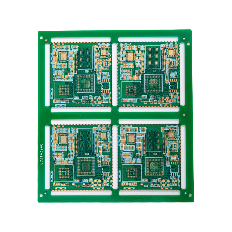
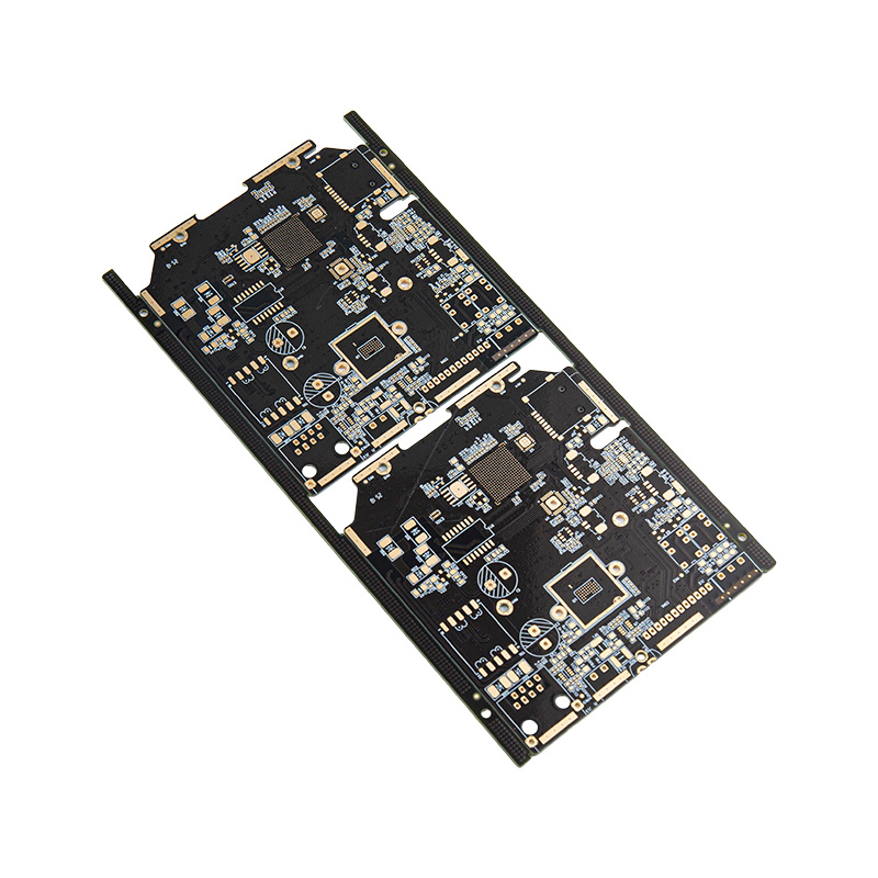
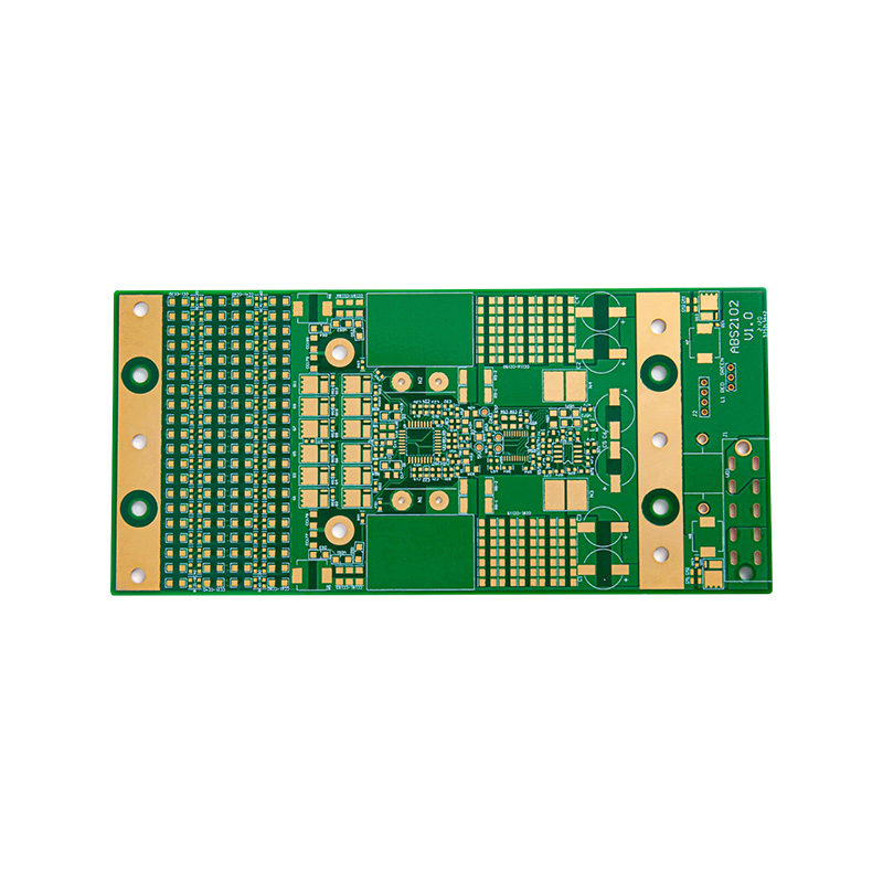
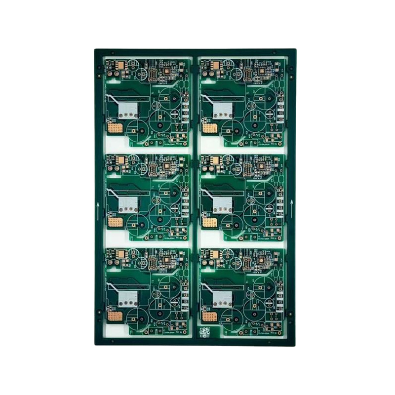
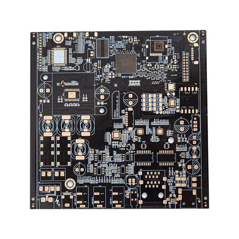
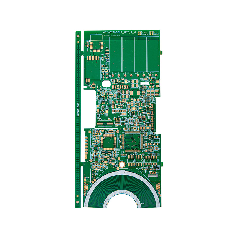
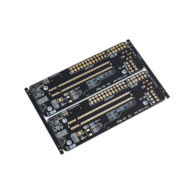
Four-Layer Double-Sided Greenened Gold Semi-Hole Plate
A four-layer double-sided PCB board, employing advanced half-hole (half-buried hole) technology and green solder mask combined with electroless gold plating (ENIG) surface treatment, is specifically designed for high-end electronic products with strict requirements for space and reliability. Its core advantages lie in: The half-hole design achieves precise electrical connections at the module edges, significantly enhancing assembly density and integration; The electroless gold plating surface provides excellent flatness, weldability, and oxidation resistance for the pads, ensuring long-term reliability; The four-layer structure provides a stable power layer and a complete ground plane, effectively optimizing signal integrity and suppressing electromagnetic interference. This board is an ideal choice for communication modules, industrial control motherboards, high-end consumer electronics, and portable medical equipment, among others.
- Specification
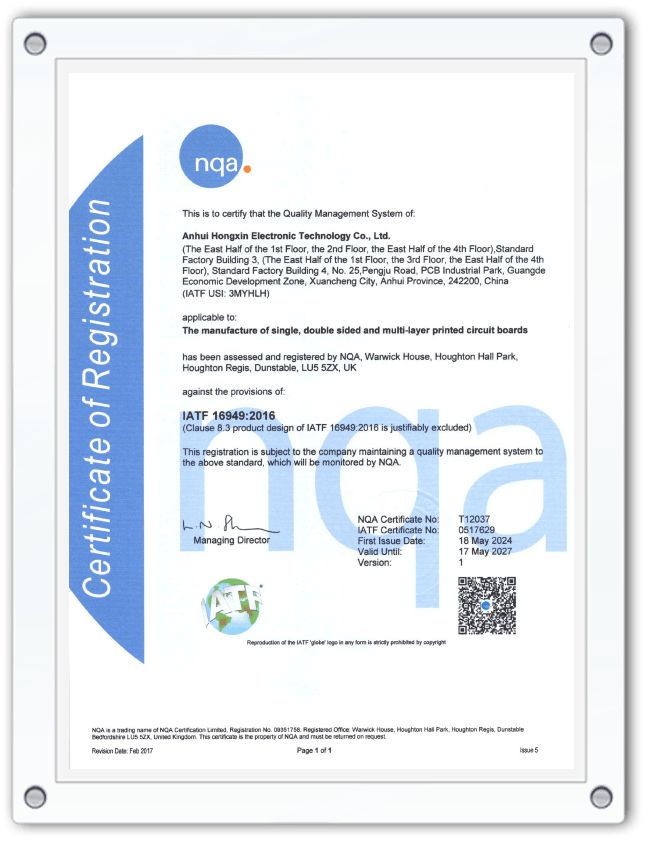
- About Hongxin
- Contact Us
|
Material |
FR-4, aluminium-based, ceramic, metal, copper-based, high-frequency, rigid-flex combined, halogen-free |
|
Board thickness |
0.3 - 6mm |
|
Copper thickness |
0.5oz - 5oz |
|
Number of layers |
1 - 32 layers |
|
Origin |
Anhui, China |
|
Surface treatment |
Ordinary tin plating, lead-free tin plating, OSP, nickel/gold plating, blue tape, silver plating, tin plating |
|
Minimum hole diameter |
0.25mm |
|
Minimum line width |
3mil (0.075mm) |
|
Minimum line spacing |
0.075mm |
|
Ratio of board thickness to hole diameter |
10:3 |


 English
  Español
  Français

