Double-Sided Greenened Gold Plate

Home / Products / PCB / Double-sided PCB / Double-Sided Greenened Gold Plate

Double-Sided Greenened Gold Plate

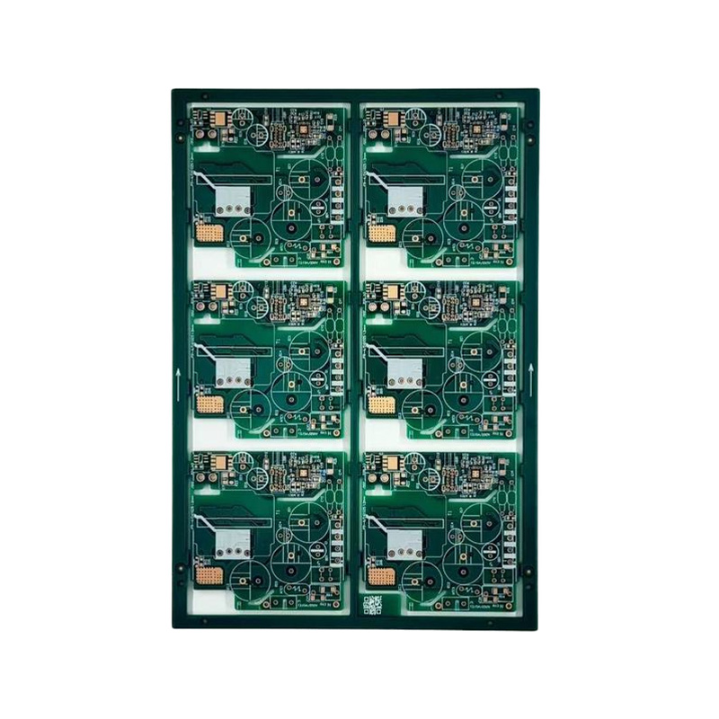
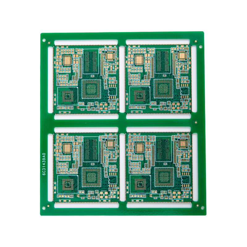
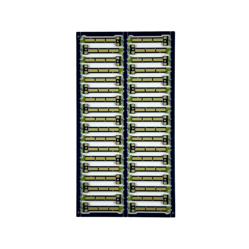
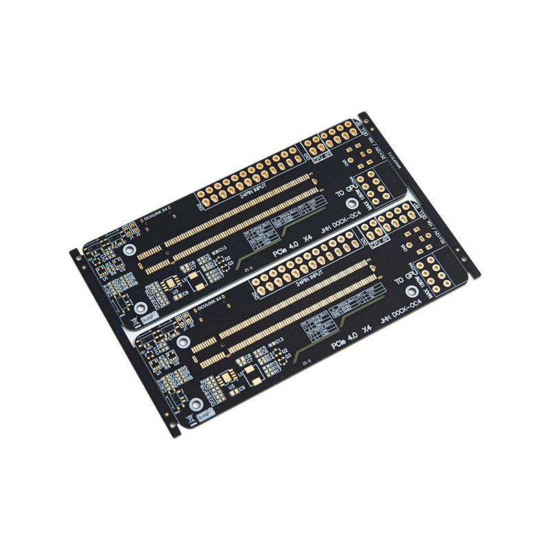
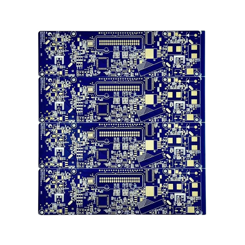
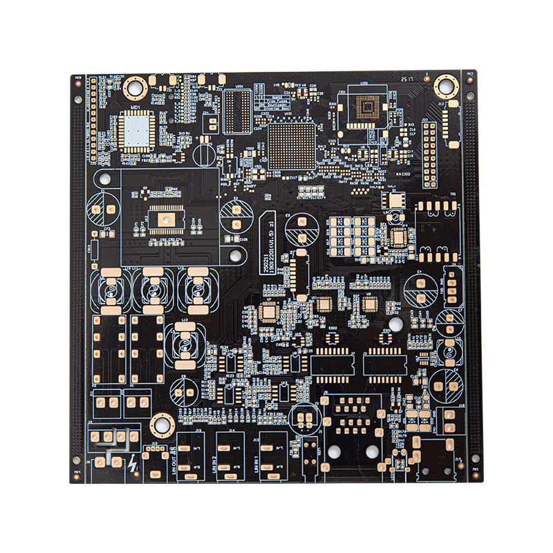
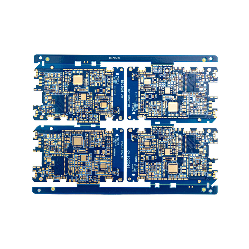
Double-sided greenized gold plated board, using vacuum precision gold plating technology, the gold plating surface adopts ultra-thin uniform coating technology, with the gold layer thickness precisely controlled within 0.05 - 0.1 μm. This not only maintains excellent conductivity and solderability, but also significantly reduces the cost of precious metals. After high-temperature aging tests, it still shows no oxidation or color change. The board body selects high insulation FR-4 base material, combined with an optimized grounding layer design, effectively suppressing electromagnetic interference. It supports stable transmission of industrial-grade medium-low speed signals and is compatible with through-hole and surface-mount hybrid packaging, meeting the integration requirements of various types of components. It is suitable for industrial control auxiliary boards, smart home sensor modules, batch consumer electronic interface boards, front-end circuits of security monitoring, etc. It is a cost-effective PCB solution that balances production economy, production efficiency, and usage stability.

Contact Us
  • Specification
  • About Hongxin
  • Contact Us

Material

 FR-4, aluminium-based, ceramic, metal, copper-based, high-frequency, rigid-flex combined, halogen-free

Board thickness

 0.3 - 6mm

Copper thickness

 0.5oz - 5oz

Number of layers

 1 - 32 layers

Origin

 Anhui, China

Surface treatment

 Ordinary tin plating, lead-free tin plating, OSP, nickel/gold plating, blue tape, silver plating, tin plating

Minimum hole diameter

 0.25mm

Minimum line width

 3mil (0.075mm)

Minimum line spacing

 0.075mm

Thickness-to-diameter ratio of holes

 10:17

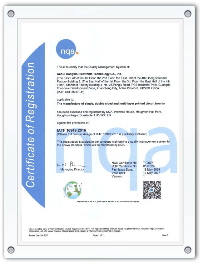
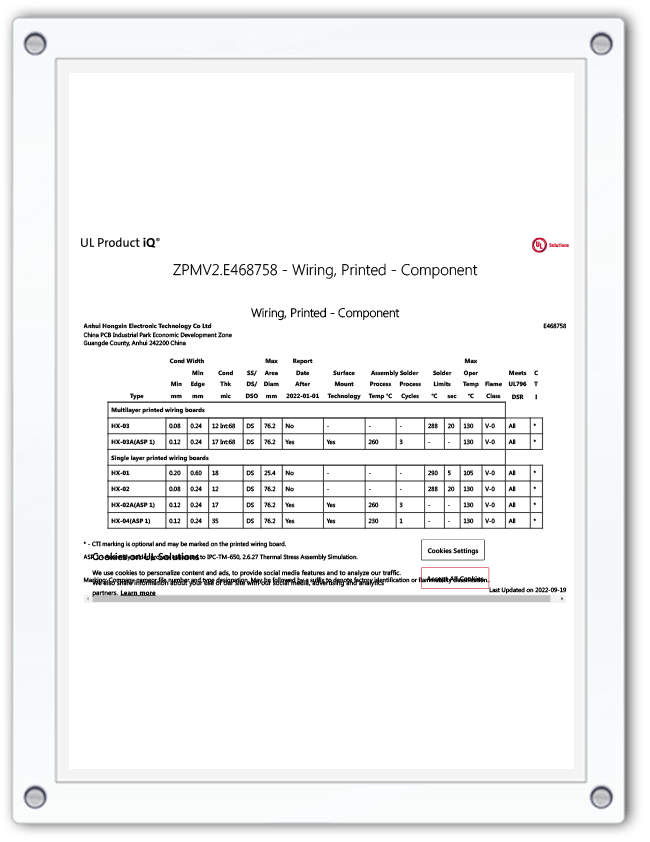
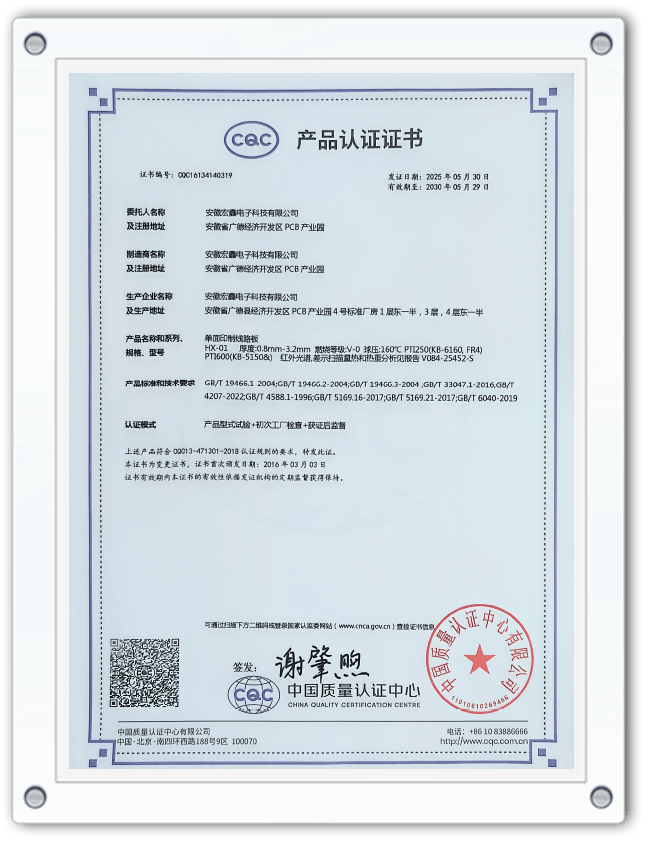
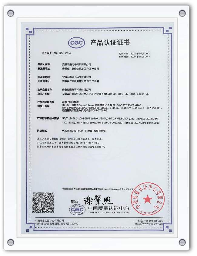
Anhui Hongxin Electronic Technology Co., Ltd. located in China P C B Industrial Park, Guangde Economic Development District, Anhui Province. Established in October 2 0 1 3, our factory occupied 2000 square meters and employs 158 staff members, including over 7 professional engineers with more than 15 years of experience. The company's P C B products include 1- 32 layer boards, high Tg boards, thick copper boards, rigid-flex boards, high- frequency boards, hybrid dielectric laminated boards, buried via boards, metal-based boards, and halogen- free boards. High-precision P C B rapid prototyping is available, with bulk orders for single and double -sided boards delivered within 6 - 7 days, 4 - 8 layer boards within 9 - 20 days, 10 - 16 layer boards within 20 - 25 days, 16 - 32 layer boards within 25 - 45 days, H D I boards within 25 days, and double- sided prototyping deliverable as quickly as 24 hours. We are committed to providing high-quality products and professional services to global customers, and we have the capability to deliver orders of both large quantities and small batches. The surface treatment processes of our products are complete. The base material types include FR-1, 22F, CEM-1, CEM-3, FR-4 (with high Tg, halogen-free, etc.), high-frequency boards, and metal substrates. All product types have passed ISO9001, ISO14001, ISO45001, IATF16949 international quality management system certifications and UL safety certifications. Our sales network extends from inland areas to Southeast Asia and Europe and America. In the fierce market competition, we have always received high praise from customers.
About
Anhui Hongxin Electronic Technology Co., Ltd.
Anhui Hongxin Electronic Technology Co., Ltd. located in China P C B Industrial Park, Guangde Economic Development District, Anhui Province. Established in October 2 0 1 3, our factory occupied 8, 413 square meters and employs 158 staff members, including over 7 professional engineers with more than 15 years of experience. The company's P C B products include 1- 32 layer boards, high Tg boards, thick copper boards, rigid-flex boards, high- frequency boards, hybrid dielectric laminated boards, buried via boards, metal-based boards, and halogen- free boards. High-precision P C B rapid prototyping is available, with bulk orders for single and double -sided boards delivered within 6 - 7 days, 4 - 8 layer boards within 9 - 20 days, 10 - 16 layer boards within 20 - 25 days, 16 - 32 layer boards within 25 - 45 days, H D I boards within 25 days, and double- sided prototyping deliverable as quickly as 24 hours. We are committed to providing high-quality products and professional services to global customers, and we have the capability to deliver orders of both large quantities and small batches. The surface treatment processes of our products are complete. The base material types include FR-1, 22F, CEM-1, CEM-3, FR-4 (with high Tg, halogen-free, etc.), high-frequency boards, and metal substrates. All product types have passed ISO9001, ISO14001, ISO45001, IATF16949 international quality management system certifications and UL safety certifications. Our sales network extends from inland areas to Southeast Asia and Europe and America. In the fierce market competition, we have always received high praise from customers.
News
Double-sided PCB Industry knowledge