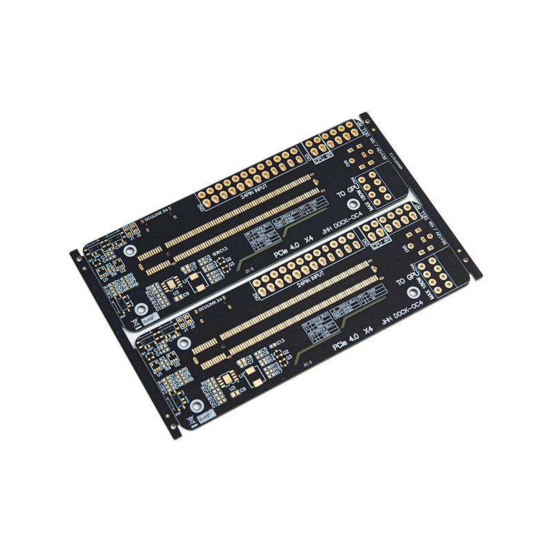
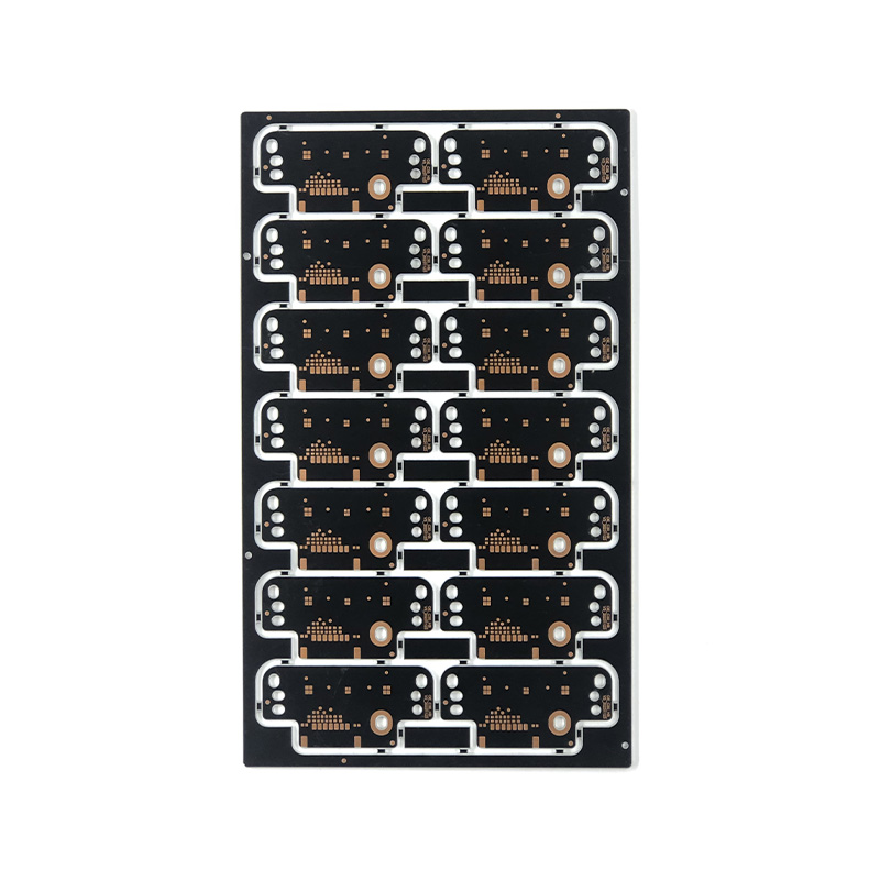
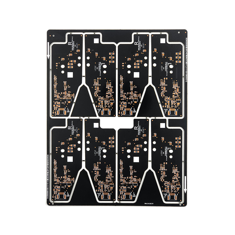
Double-Sided Gold-Plated PCB
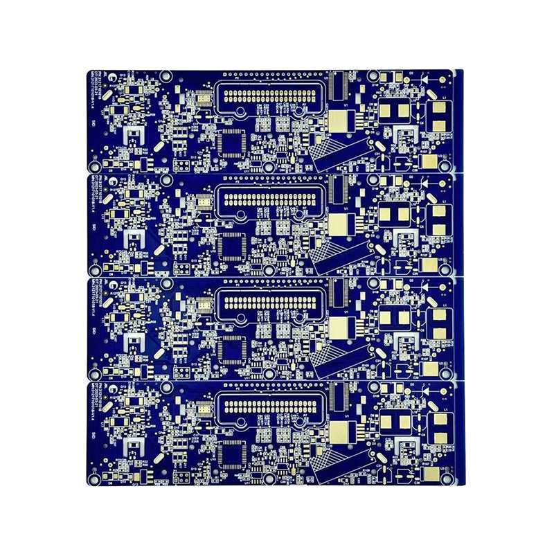
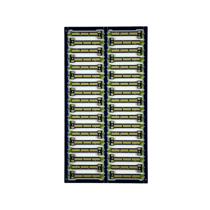
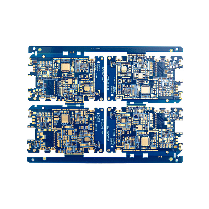
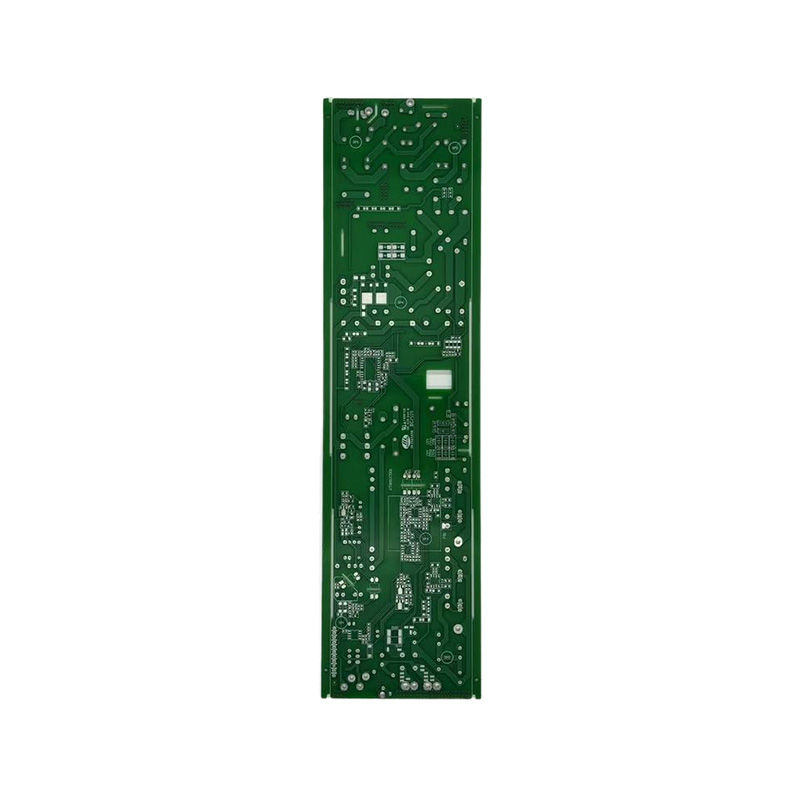
Double-sided gold-plated PCBs utilize an electroless immersion gold (ENIG) process to create uniform gold and nickel layers on both sides of the PCB. This process combines excellent oxidation resistance, flatness, and solderability, making it particularly suitable for high-precision, high-reliability electronic devices. The gold-plated layer is wear-resistant and corrosion-resistant, making it suitable for multiple reflow soldering cycles and wire bonding. It is widely used in communications equipment, industrial control motherboards, medical equipment, and high-end consumer electronics. This process eliminates issues such as uneven tin spraying and the susceptibility of OSP to oxidation, while also supporting fine-pitch BGA and QFN packages, making it an ideal choice for high-performance PCBs.
- Specification
- About Hongxin
- Contact Us
|
Material |
FR-4 |
|
Supplier |
Shengyi |
|
Board Thickness |
1.6mm |
|
Finished Copper Thickness |
36µm |
|
Solder Mask |
Royal Blue |
|
Texture |
White |
|
Surface Treatment |
Gold |
|
Finished Dimensions |
199mm x 180mm |
|
Trace Width |
0.15mm |
|
Trace Spacing |
0.12mm |
|
Minimum Hole |
0.3mm |


 English
  Español
  Français

