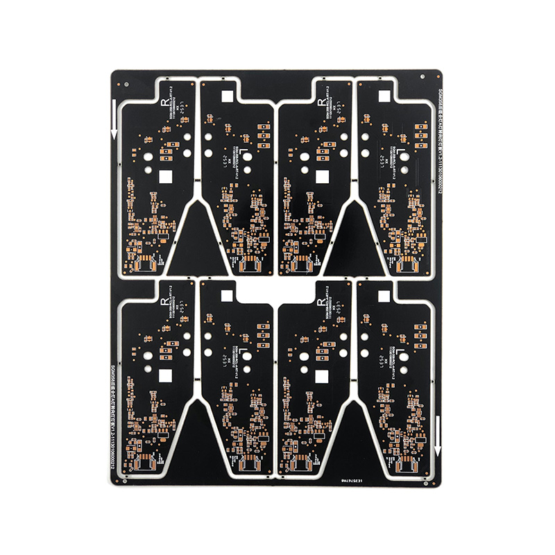
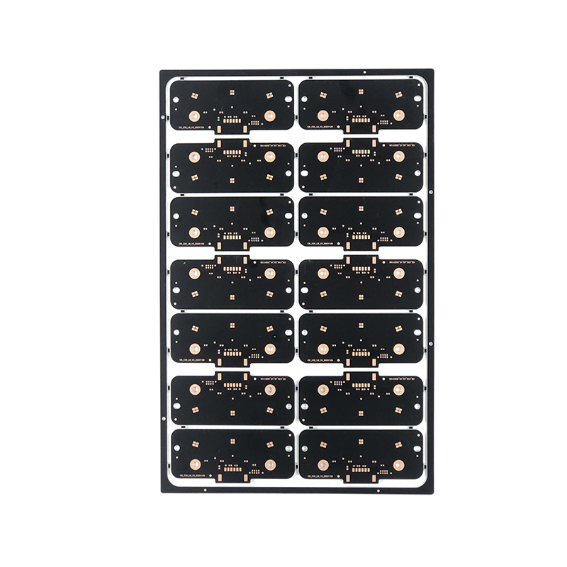
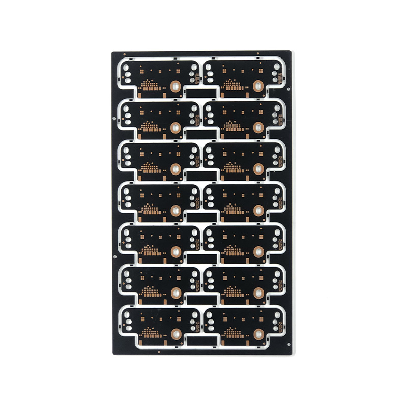
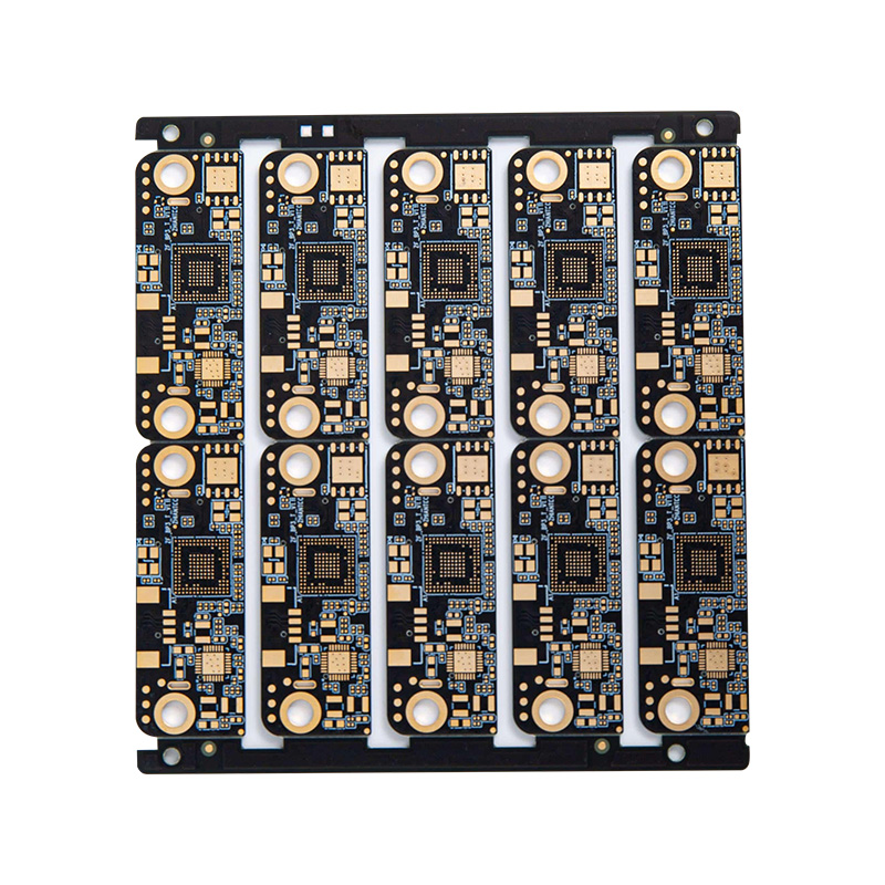
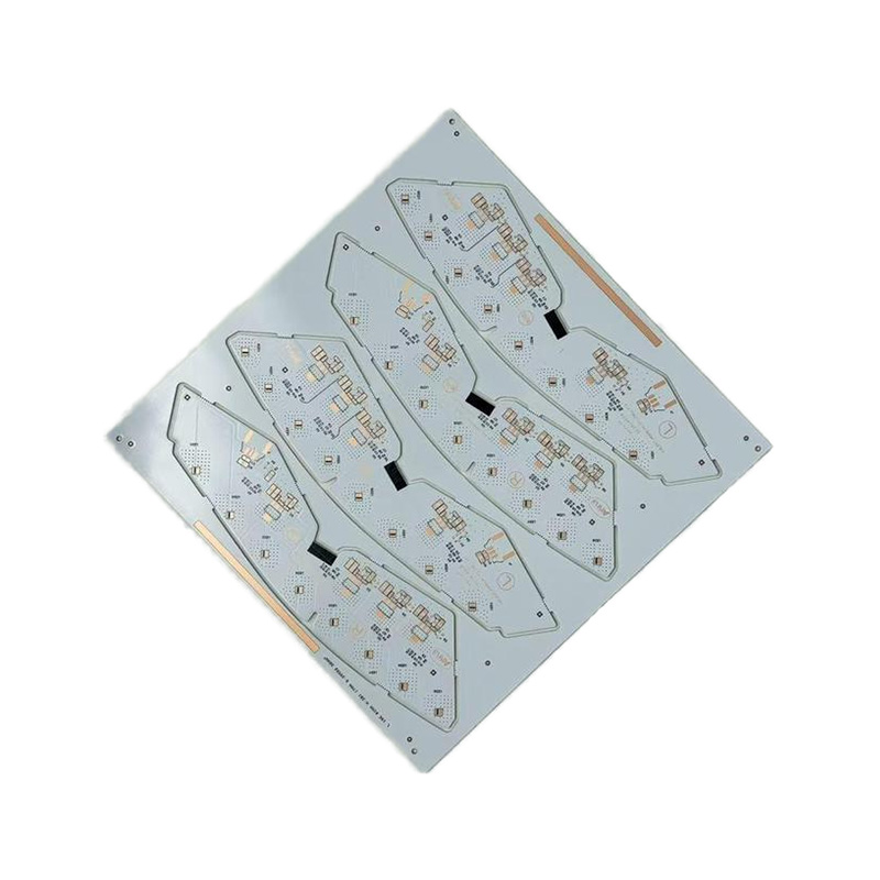
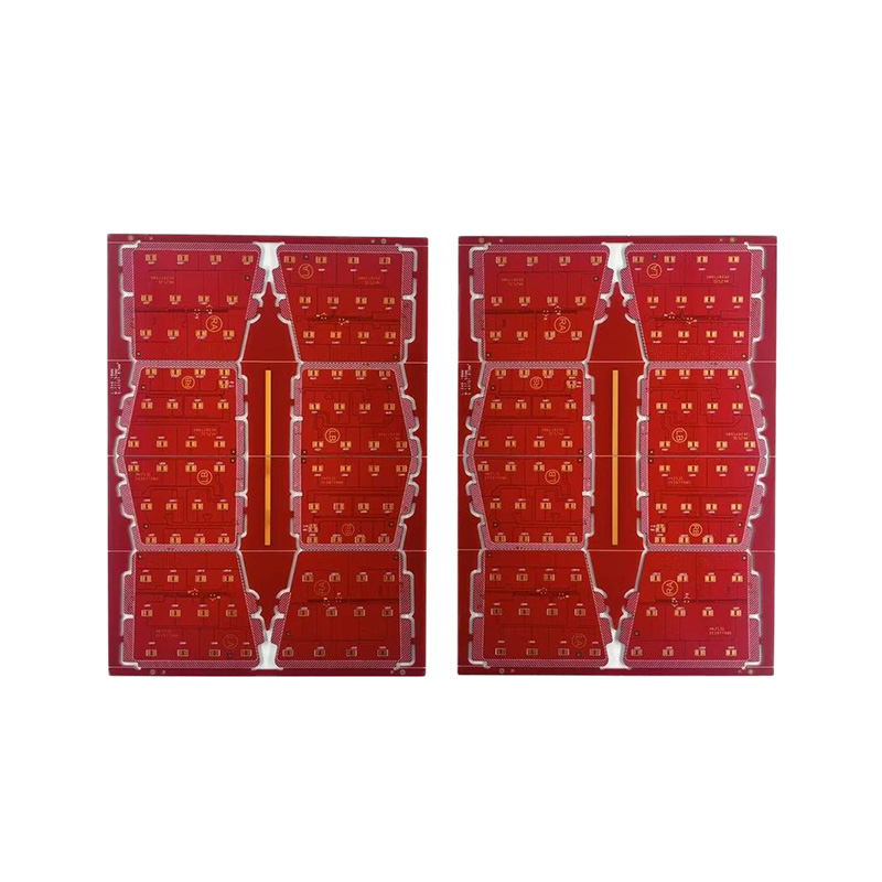
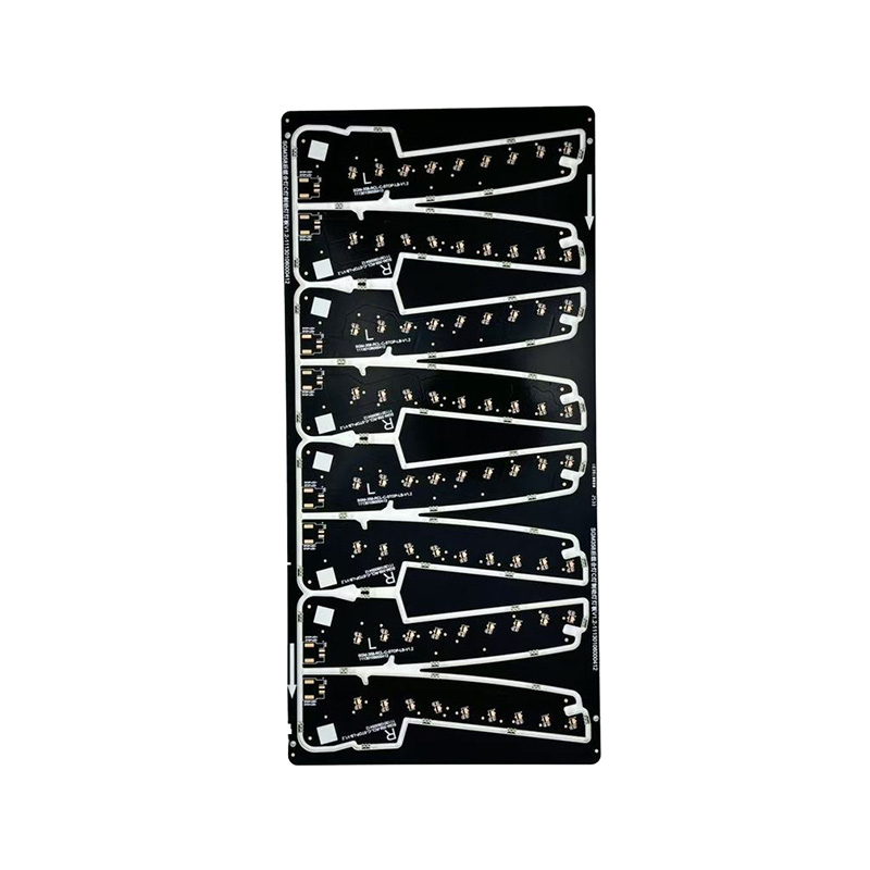
Double-Sided Black OSP PCB Board
Double-sided black OSP PCB board with matte black solder mask layer and uniform OSP surface treatment: The black layer not only achieves line concealment, but also has low reflectivity, which is suitable for the visual inspection process of precision equipment. The OSP coating layer is formed by precise thickness control to form a dense protective film. The board body integrates "R/L" direction marking, positioning slots and process dividing edges, which are suitable for high-speed mounting and precise cutting of automated production lines. The circuit design supports 2.5mil/2.5mil fine line width and spacing, combined with 0.25mm micro via holes, is compatible with high-integration chip packaging, and at the same time uses high Tg (170℃) FR-4 substrate. It is suitable for core modules of smart wearables, portable audio equipment circuits, etc., which have requirements for structure, yield, and cost.
- Specification
- About Hongxin
- Contact Us
|
Material |
FR-4, aluminium-based, ceramic, metal, copper-based, high-frequency, rigid-flex combined, halogen-free |
|
Board thickness |
0.3 - 6mm |
|
Copper thickness |
0.5oz - 5oz |
|
Number of layers |
1 - 32 layers |
|
Origin |
Anhui, China |
|
Surface treatment |
Ordinary tin plating, lead-free tin plating, OSP, nickel/gold plating, blue tape, silver plating, tin plating |
|
Minimum hole diameter |
0.25mm |
|
Minimum line width |
3mil (0.075mm) |
|
Minimum line spacing |
0.075mm |
|
Thickness-to-diameter ratio of holes |
10:10 |


 English
  Español
  Français

