

 English
  Español
  Français
How to Choose the Right Multilayer PCB for High-Density Applications?
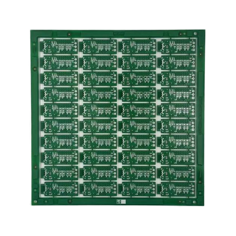
The evolution of modern electronics towards miniaturization and increased functionality has placed unprecedented demands on printed circuit boards (PCBs). In this landscape, the Multilayer PCB has become the cornerstone of high-density applications, from advanced telecommunications and high-speed computing to compact medical devices. Unlike simpler boards, a multilayer PCB integrates multiple conductive layers separated by insulating materials, allowing for complex routing and higher component density in a confined space. However, selecting the optimal one is not a one-size-fits-all process. It requires a nuanced understanding of your application's specific electrical, thermal, and physical requirements. This guide will delve into the critical factors and trade-offs involved in making an informed choice for your high-density design.
Content
- 1 1. Understanding Your Application's Core Requirements
- 2 2. Critical Technical Specifications for Selection
- 3 3. The Role of Advanced Manufacturing Techniques
- 4 4. Cost vs. Performance Trade-offs and Decision Framework
- 5 FAQ
- 5.1 What is the main difference between a standard multilayer PCB and an HDI PCB?
- 5.2
- 5.3 How do I know if my design needs a specialized material like a low-loss laminate instead of standard FR-4?
- 5.4 What are the key factors that drive the cost of a high-density multilayer PCB?
- 5.5 Can I mix different materials in a single multilayer PCB stack-up?
- 5.6 How important is the "stack-up" design, and what are the consequences of a poor stack-up?
1. Understanding Your Application's Core Requirements
Before diving into material specs or layer counts, a thorough analysis of your end application is paramount. High-density applications are defined by their need to pack significant functionality into a small footprint, but the underlying drivers can vary greatly. For instance, a high-frequency RF module prioritizes signal integrity and low loss, while a powerful processor board focuses on heat dissipation and power integrity. Start by defining the primary purpose: Is it for ultra-high-speed data transfer, power-hungry processing, or operation in harsh environments? The answers will directly dictate your choice in substrate material, layer stack-up, and manufacturing tolerances. Neglecting this foundational step can lead to over-engineering and unnecessary cost or, worse, an underperforming product that fails in the field. A successful selection balances performance, reliability, and cost-effectiveness by aligning the PCB's capabilities with the application's non-negotiable demands.
- Signal Speed and Integrity: Determine the maximum frequency and edge rates of your signals. High-speed designs require careful consideration of dielectric constant (Dk) and dissipation factor (Df).
- Power Requirements: Analyze current loads. High-power applications need thicker copper weights and may require dedicated power and ground planes for stable delivery.
- Thermal Management: Evaluate the heat generated by components. This influences the choice of substrate material (e.g., high Tg, thermal conductivity) and the potential need for thermal vias or metal cores.
- Environmental Factors: Consider operating temperature range, humidity, and exposure to chemicals or vibration. This affects material selection and conformal coating requirements.
- Size and Weight Constraints: Define the exact physical dimensions and weight limits, which directly impact the feasible layer count and via technologies like High-Density Interconnect (HDI) structures.
2. Critical Technical Specifications for Selection
With application requirements clear, the focus shifts to the technical specifications that transform those needs into a physical board. This is where the detailed engineering begins. Key parameters like layer count, material properties, and copper weight interact in complex ways to define the PCB's performance envelope. For example, increasing layer count improves routing density but adds cost and can complicate impedance control. Choosing a low-loss laminate is excellent for high-speed signals but comes at a premium. Understanding these specifications in depth allows you to make strategic decisions, optimizing the board for its specific role without compromising on critical performance aspects or inflating the budget. This section breaks down the most consequential specs you must evaluate.
2.1 Layer Count and Stack-up Configuration
The number of layers and their arrangement (stack-up) is the most fundamental decision in multilayer PCB design. It determines routing capability, signal integrity, and EMI performance. A well-planned stack-up uses symmetrical construction to prevent warping and strategically places power and ground planes to provide shielding and stable reference planes for high-speed signals. For moderate complexity, an 8-layer board often offers a good balance. For extreme density, designers turn to HDI (High-Density Interconnect) PCB design techniques, which utilize microvias and buried/blind vias to achieve routing escape for fine-pitch BGAs and other advanced components. The stack-up is not just about adding layers; it's about assigning each layer a specific purpose (e.g., signal, plane, mixed) to create a predictable electromagnetic environment.
- 4-8 Layers: Suitable for many industrial and consumer applications with moderate component density.
- 8-16 Layers: Common in networking equipment, data storage, and advanced medical devices requiring complex routing.
- 16+ Layers & HDI: Essential for aerospace, high-end servers, and compact wearable technology where space is at an absolute premium.
| Layer Count Range | Primary Benefit | Typical Use Case |
| 4-6 Layers | Cost-effective, good for controlled impedance | Automotive ECUs, consumer IoT devices |
| 8-12 Layers | Excellent signal integrity and power distribution | Switches, routers, data acquisition systems |
| 12+ Layers with HDI | Maximum density and miniaturization | Smartphones, military comms, implantable medical devices |
2.2 Material Selection: Beyond Standard FR-4
While standard FR-4 is the workhorse for many applications, high-density and high-performance designs often demand specialized materials. The base material, or laminate, governs electrical performance (Dk, Df), thermal reliability (Tg, Td), and mechanical stability. For digital circuits with speeds above 1-2 GHz or analog RF circuits, the signal loss in standard FR-4 can be prohibitive. This is where understanding options for a multilayer PCB for RF and microwave applications becomes critical. Materials like Rogers, Isola, or specialized halogen-free FR-4 variants offer lower loss and more stable Dk over frequency and temperature. Similarly, applications in high-temperature environments require laminates with a high Glass Transition Temperature (Tg) to maintain structural integrity during operation and soldering.
- Standard FR-4: Cost-effective, good mechanical strength. Best for digital applications below ~1 GHz and where thermal stress is low.
- Mid-Loss / High-Performance FR-4: Improved Df and thermal properties (Tg > 170°C). Suitable for faster digital and some RF applications.
- Low-Loss / RF Laminates: Very low Df, stable Dk. Essential for high-frequency multilayer PCB designs in radar, 5G, and satellite systems.
- High-Tg & Halogen-Free: Enhanced thermal and environmental reliability. Used in automotive, down-hole drilling, and green electronics.
| Material Class | Typical Df (10 GHz) | Key Advantage | Trade-off |
| Standard FR-4 | 0.020 | Lowest cost, widely available | High loss, poor performance at high freq/heat |
| High-Tg FR-4 | 0.015 | Better thermal resistance, good value | Loss still high for critical RF |
| Low-Loss Laminate | 0.003 - 0.005 | Superior signal integrity for high-speed design | Cost can be 5-10x standard FR-4 |
| Ceramic-filled PTFE | 0.001 - 0.002 | Ultra-low loss, ideal for mmWave | Very high cost, challenging fabrication |
3. The Role of Advanced Manufacturing Techniques
Choosing the right specifications is only half the battle; realizing them depends on advanced manufacturing capabilities. As feature sizes shrink and densities increase, traditional PCB fabrication reaches its limits. This is where technologies like High-Density Interconnect (HDI), advanced via structures, and stringent controlled impedance fabrication come into play. These techniques directly enable the creation of reliable high-density interconnect PCB assemblies that can host modern, fine-pitch components like BGA packages with over 1000 pins. Partnering with a manufacturer that masters these processes is crucial, as the manufacturing precision directly affects yield, performance, and long-term reliability. This section explores the key manufacturing considerations that impact the final quality of your multilayer board.
- HDI Technology: Employs microvias (≤ 150µm), blind/buried vias, and sequential lamination to create more interconnect paths in less space, which is a cornerstone of HDI PCB design.
- Controlled Impedance: Requires precise control over trace width, dielectric thickness, and material Dk to match design targets (e.g., 50Ω, 100Ω differential).
- Fine Line/Space: The ability to reliably produce trace widths and spacings below 100µm (4 mils) is critical for dense routing.
- Surface Finish: Choice of finish (ENIG, Immersion Silver, HASL, etc.) affects solderability, shelf life, and signal loss at high frequencies.
4. Cost vs. Performance Trade-offs and Decision Framework
Designing a multilayer PCB for high-density applications invariably involves navigating a series of cost versus performance trade-offs. The goal is to achieve the required functionality and reliability without unnecessary expenditure. Every decision, from adding an extra layer to specifying a specialty laminate, carries a cost implication. For instance, while an HDI design offers incredible density, it significantly increases fabrication complexity and cost compared to a standard through-hole via design. A structured decision-making framework helps rationalize these choices. Start by categorizing requirements as "Mandatory," "Important," and "Nice-to-have." Allocate budget primarily to meet mandatory specs (e.g., a specific material for a multilayer PCB for RF and microwave application), then evaluate if the performance gains from "Important" items justify their cost. This disciplined approach prevents over-specification.
- Mandatory Drivers: These are non-negotiable for function or compliance (e.g., operating frequency, thermal rating, reliability standards). Cost is secondary here.
- Performance Enhancers: Features that improve signal integrity, power delivery, or thermal performance but have acceptable alternatives (e.g., a mid-loss vs. low-loss material). Analyze cost-benefit carefully.
- Geometric Drivers: Requirements driven purely by size and form factor, such as needing HDI to fit a board into a tiny enclosure. Explore if mechanical redesign can relax these constraints before committing to expensive tech.
- Volume Considerations: The per-unit cost impact of advanced features decreases at very high production volumes, making premium options more justifiable.
| Design Choice | Performance Benefit | Cost Impact | When to Choose |
| Increase from 8 to 10 layers | Better signal isolation, more routing channels | Moderate increase (~15-25%) | When facing severe routing congestion or EMI issues |
| Switch from FR-4 to Low-Loss Laminate | Reduced signal attenuation, faster edge rates | High increase (100-500%) | Mandatory for signal integrity in high-frequency multilayer PCB applications |
| Adopt HDI with Microvias | Enables miniaturization, escapes fine-pitch BGAs | Very High increase (30-100%) | When size/weight is a mandatory constraint and component density demands it |
| Specify 2oz vs. 1oz Copper | Higher current capacity, better thermal conduction | Low-Moderate increase (~5-15%) | For power sections or boards with high thermal loads |
FAQ
What is the main difference between a standard multilayer PCB and an HDI PCB?
The core difference lies in the density of the interconnections and the via technology used. A standard Multilayer PCB primarily uses through-hole vias that span the entire board thickness, along with potentially larger trace widths/spacings. An HDI (High-Density Interconnect) PCB employs advanced microvias (typically laser-drilled and less than 150µm in diameter), blind vias (connecting an outer layer to an inner layer), and buried vias (connecting inner layers only). This allows for many more connection points in a given area, enabling the routing of high-pin-count components like modern processors and FPGAs. HDI is not just about more layers; it's about a more efficient use of space within those layers, making it essential for the most compact and complex devices like smartphones and advanced medical implants.
How do I know if my design needs a specialized material like a low-loss laminate instead of standard FR-4?
This decision hinges primarily on your signal's frequency and your acceptable loss budget. As a rule of thumb, if your design involves digital signals with edge rates corresponding to fundamental frequencies above 1-2 GHz, or specifically deals with RF/analog signals in the hundreds of MHz to GHz range, standard FR-4's higher dissipation factor (Df) will cause significant signal attenuation and integrity issues. This is critical for a multilayer PCB for RF and microwave use. Evaluate your link budget: calculate the total loss from trace length, connectors, and the PCB dielectric. If the loss from FR-4 jeopardizes your noise margin or system gain, a low-loss laminate becomes necessary. Additionally, if your application requires stable impedance over a wide frequency band, low-loss materials with stable Dk are mandatory.
What are the key factors that drive the cost of a high-density multilayer PCB?
Cost drivers for complex multilayer boards are multifaceted. The primary factors include: Layer Count (more layers increase material and processing time), Board Size (larger boards use more raw material), Material Type (specialty low-loss or high-Tg laminates cost significantly more than standard FR-4), and Manufacturing Technology (utilizing HDI PCB design with laser drilling and sequential lamination adds substantial cost). Secondary but important factors are: Minimum Trace/Width and Via Size (finer features require more precise, lower-yield processes), Controlled Impedance Requirements (adds testing and tighter process control), Surface Finish (e.g., ENIG is more expensive than HASL), and Order Volume (prototypes are much more expensive per unit than large production runs). Understanding these levers allows for cost-optimization discussions with your manufacturer.
Can I mix different materials in a single multilayer PCB stack-up?
Yes, this technique is known as a hybrid or mixed-material stack-up and is increasingly common in sophisticated high-density interconnect PCB assemblies. The primary reason to do this is cost-performance optimization. For example, a design might use low-loss Rogers material for the top and bottom layers where critical RF traces are routed, while using standard or mid-loss FR-4 for the inner signal and power layers. This provides excellent RF performance where needed while controlling overall cost. However, hybrid stack-ups introduce significant manufacturing complexity. The different materials have different thermal expansion coefficients (CTEs) and lamination properties, which can challenge reliability if not handled expertly. They also require careful planning of via structures that transition between materials. This approach should be undertaken in close collaboration with an experienced PCB fabricator.
How important is the "stack-up" design, and what are the consequences of a poor stack-up?
The stack-up design is arguably the most critical aspect of a successful high-frequency multilayer PCB or any high-speed digital board. It defines the electrical behavior of the board before a single component is placed. A good stack-up ensures proper impedance control, minimizes crosstalk and electromagnetic interference (EMI), provides stable power delivery with low inductance, and prevents mechanical warpage. The consequences of a poor stack-up are severe: Signal Integrity Problems (excessive ringing, reflections, crosstalk causing data errors), Power Integrity Issues (voltage droop and ground bounce leading to circuit malfunction), Radiated EMI (failing regulatory compliance tests), and Mechanical Failure (warping during assembly causing poor solder joints). Investing time in a properly engineered, symmetrical stack-up with dedicated power and ground planes is essential for first-pass success.


 LET'S CREATE THE FUTURE TOGETHER

Contact Us Anytime
Copyright © Anhui Hongxin Electronic Technology Co., Ltd. All Rights
Reserved.
privacy
Wholesale Printed Circuit Board Suppliers, Manufacturers
![]()
