

 English
  Español
  Français
PCB Assembly Explained: Process Flow, Soldering Methods & Testing
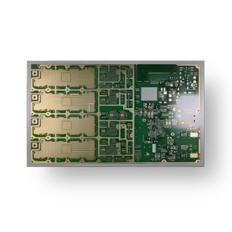
PCB assembly (often abbreviated PCBA) is the process of populating a bare printed circuit board with electronic components — resistors, capacitors, ICs, connectors — and soldering them into place to create a functional circuit. The bare board itself, sometimes called a PCB, is just a substrate with copper traces etched into it; it becomes a working device only after assembly, soldering, and testing are complete.
Content
PCB vs PCBA: Understanding the Difference
The terms "PCB" and "PCBA" are often used interchangeably but refer to different stages of the same product. A PCB (printed circuit board) is the unpopulated board itself — layers of fiberglass or other substrate material with copper conductive paths, solder mask, and silkscreen markings, but no components attached. A PCBA (printed circuit board assembly) is that same board after all required components have been mounted and soldered, ready to be installed into a final product or tested as a standalone circuit.
This distinction matters when sourcing manufacturing services, since "PCB manufacturing" typically refers only to fabricating the bare board, while "PCB assembly" or "PCBA service" includes component sourcing, placement, and soldering on top of that fabricated board.
The PCB Manufacturing and Assembly Process Flow
A complete PCB-to-PCBA process generally follows a sequence of distinct stages, each with its own quality checkpoints before the board moves to the next step:
- Design and DFM review: The circuit design (schematic and layout files, typically Gerber format) is checked for manufacturability — trace widths, hole sizes, and component spacing must meet the fabricator's capabilities.
- Bare board fabrication: Copper layers are etched, layers are laminated together for multilayer boards, holes are drilled and plated, solder mask and silkscreen are applied, and the board is cut to its final shape.
- Solder paste application: For surface-mount assembly, solder paste is applied to the pads through a stencil using a screen printer, creating precise deposits at every component location.
- Component placement: A pick-and-place machine positions surface-mount components onto the wet solder paste using vacuum nozzles, guided by the placement program generated from the design files.
- Reflow soldering: The populated board passes through a reflow oven with multiple temperature zones, melting the solder paste to form permanent electrical and mechanical connections, then cooling to solidify the joints.
- Through-hole component insertion and wave/hand soldering: Larger components with leads that pass through drilled holes are inserted, then soldered either by wave soldering (the board passes over a wave of molten solder) or by hand for low-volume or sensitive components.
- Inspection and testing: Automated optical inspection (AOI), X-ray inspection for hidden joints (such as BGA packages), and functional or in-circuit testing verify the assembly meets specification.
- Final cleaning and packaging: Flux residue is cleaned if required, and boards are packaged — often in anti-static bags or trays — for shipping or further integration.
SMT vs Through-Hole Soldering: Choosing the Right Method
Most modern PCB assemblies combine two soldering approaches, and understanding when each is used helps explain why a single board often goes through multiple soldering steps rather than just one.
| Method | Component Type | Best Suited For |
|---|---|---|
| SMT (Surface-Mount Technology) | Small components mounted directly on pads (resistors, capacitors, ICs, BGAs) | High-density, automated, high-volume production |
| THT (Through-Hole Technology) | Leaded components inserted through drilled holes (connectors, transformers, large capacitors) | Mechanically stressed connections, high-power components |
Connectors, switches, and components subject to repeated mechanical stress (such as plugging and unplugging cables) are commonly through-hole even on otherwise SMT-dominant boards, because the leads passing through the board provide significantly stronger mechanical anchoring than surface-mount pads alone.
Inspection and Testing Methods Used in PCB Assembly
Quality control isn't a single step at the end of the line — it's built into multiple checkpoints throughout assembly, since catching a defect early (such as a solder paste application error) is far cheaper than discovering it after full assembly.
- Solder paste inspection (SPI): Checks paste volume and placement immediately after stencil printing, before components are placed
- Automated optical inspection (AOI): Uses cameras to verify component presence, orientation, and solder joint quality after placement and reflow
- X-ray inspection: Necessary for components with hidden solder joints underneath the package, such as ball grid array (BGA) chips, where AOI cannot see the connection
- In-circuit testing (ICT): Uses a bed-of-nails fixture to verify electrical connectivity and component values against the design specification
- Functional testing (FCT): Powers the board and verifies it performs its intended function, simulating real-world operating conditions
From Bare Board to Working Circuit: How a Finished PCB Gets Used
Once a PCB assembly is complete, "using" it depends on the role it plays in the final product. A finished PCBA can function as a standalone control board (such as a power supply module), or it can be integrated into a larger product enclosure where it connects to other boards, displays, or input/output components via connectors and ribbon cables.
Practical steps for integrating an assembled PCB into a system typically include:
- Mounting the board securely using the designated mounting holes, with standoffs or spacers to prevent the underside copper from contacting a conductive enclosure
- Connecting power input according to the voltage and polarity markings on the board — reversed polarity is one of the most common causes of immediate board failure on first power-up
- Verifying signal connectors and headers match the pinout documentation before connecting peripheral boards or sensors
- Performing an initial power-up check with current-limited power where possible, watching for unexpected heating on any component, which can indicate a short circuit or incorrectly placed part
For boards intended to be reprogrammed or configured (such as those with onboard microcontrollers), the assembly typically includes a programming header or test points specifically for this purpose, allowing firmware to be loaded after assembly is complete and before final functional testing.
Recommended Products


 LET'S CREATE THE FUTURE TOGETHER

Contact Us Anytime
Copyright © Anhui Hongxin Electronic Technology Co., Ltd. All Rights
Reserved.
privacy
Wholesale Printed Circuit Board Suppliers, Manufacturers
![]()
