


 English
  Español
  Français
PCB Assembly (PCBA): Process Steps, Printing & Pick and Place
Content
- 1 What Is a PCB Assembly (PCBA)?
- 2 The Core PCB Assembly Process Steps
- 3 Solder Paste Printing: Stencil vs Other Methods
- 4 Pick and Place: How Component Placement Works
- 5 Reflow Soldering and Quality Inspection
- 6 Through-Hole vs. Surface Mount Assembly
- 7 Common Challenges in PCBA Manufacturing
- 8 Choosing a PCB Assembly Partner
What Is a PCB Assembly (PCBA)?
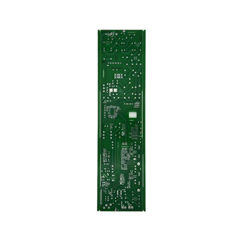
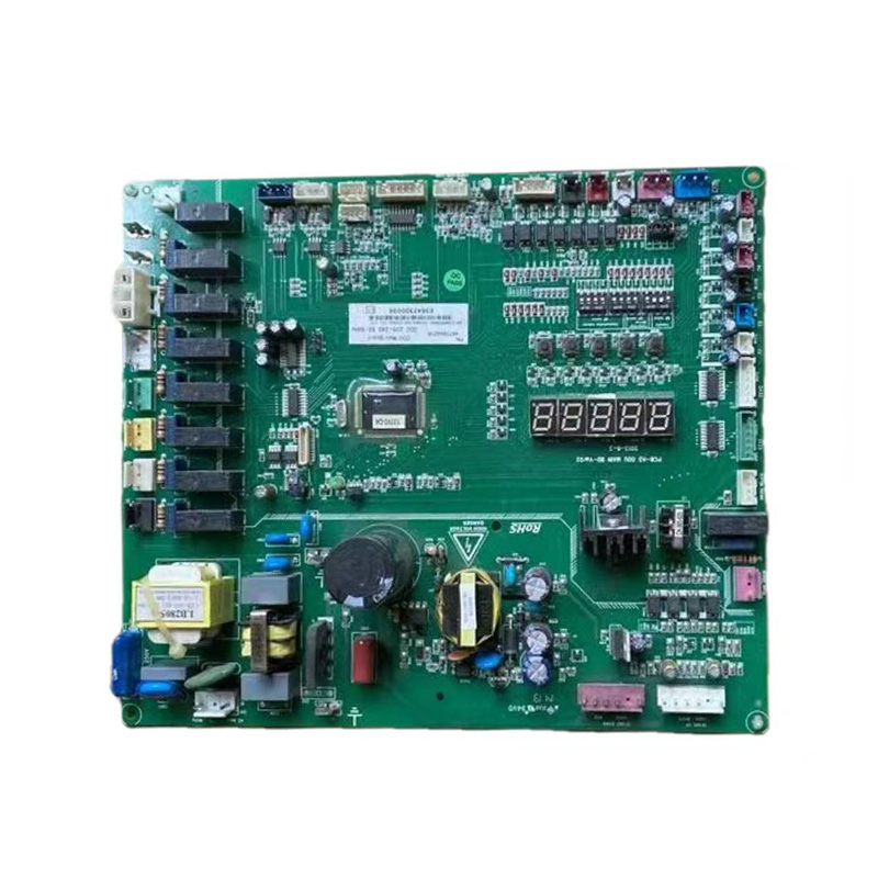
PCB assembly, or PCBA, is the process of populating a bare printed circuit board with electronic components — resistors, capacitors, ICs, connectors — and soldering them into place so the board becomes a functioning electronic circuit. A bare PCB on its own is just a patterned copper layout on a substrate; it isn't functional until components are placed and permanently bonded through soldering.
PCBA manufacturing sits downstream of PCB fabrication. Fabrication produces the bare board itself, while assembly is the separate stage where that board is turned into a working device, whether it's a single prototype or a production run of thousands of units.
The Core PCB Assembly Process Steps
While specifics vary by board complexity, most PCB assembly lines follow the same general sequence:
- Solder paste printing: Solder paste is applied to the board's pads through a stencil, creating the bonding points for surface-mount components.
- Pick and place: An automated machine places components onto the solder-pasted pads at high speed and precision.
- Reflow soldering: The populated board passes through a reflow oven, melting the solder paste to permanently bond components to the board.
- Through-hole insertion (if applicable): Components with leads are manually or automatically inserted into drilled holes and wave-soldered.
- Inspection and testing: Automated optical inspection (AOI), X-ray inspection, and functional testing verify solder joint quality and circuit performance.
Solder Paste Printing: Stencil vs Other Methods
Solder paste application is the first step in surface-mount assembly, and the method used affects both speed and precision.
| Method | Precision | Best Suited For |
|---|---|---|
| Stencil printing | High, consistent deposit volume | Mid-to-high volume production runs |
| Jet printing (dispensing) | Moderate to high, no stencil needed | Prototypes, low-volume or frequently changing designs |
Pick and Place: How Component Placement Works
Pick and place machines use vacuum nozzles mounted on a high-speed gantry or rotary head to lift components from feeder reels or trays and position them precisely on the board's solder-pasted pads. Modern machines use vision systems to verify component orientation and pad alignment before placement, correcting for minor rotational or positional errors in real time.
Placement speed and accuracy scale with machine class — high-speed chip shooters handle small passive components like resistors and capacitors at very high throughput, while slower, higher-precision placement heads handle fine-pitch ICs and connectors where positioning tolerance is much tighter.
Reflow Soldering and Quality Inspection
After placement, boards move through a reflow oven with multiple temperature zones — preheat, soak, reflow, and cooling — following a profile calibrated to the specific solder paste alloy and board thermal mass. An incorrect reflow profile is one of the most common causes of solder defects like tombstoning or cold joints.
Following reflow, inspection typically includes automated optical inspection to catch visible defects (missing components, misalignment, bridging), and X-ray inspection for solder joints hidden under components like BGAs where visual inspection alone can't confirm joint quality.
Through-Hole vs. Surface Mount Assembly
Most modern boards use a combination of both technologies rather than exclusively one:
- Surface mount technology (SMT): Components sit directly on the board surface, enabling smaller components and higher placement density — the dominant method for modern electronics.
- Through-hole technology (THT): Component leads pass through drilled holes and are soldered on the opposite side, offering stronger mechanical bonds — still used for connectors and components under mechanical stress.
Common Challenges in PCBA Manufacturing
- Component sourcing and obsolescence: Long lead times or discontinued parts can stall production and require design substitutions.
- Fine-pitch component placement: As component pitch shrinks, placement tolerance and paste volume control become significantly more critical.
- Thermal management during reflow: Boards with mixed component sizes and thermal masses need carefully tuned reflow profiles to avoid under- or over-heating different areas.
- Traceability requirements: Industries like automotive and medical often require full component-lot traceability, adding documentation overhead to the assembly process.
Choosing a PCB Assembly Partner
A few practical questions help evaluate a potential assembly partner:
- What inspection methods are standard versus optional, and is X-ray inspection available for BGA and fine-pitch components?
- What is the minimum order quantity, and can the line handle both prototype runs and full production volume?
- Does the partner offer component sourcing, or is it assembly-only requiring the customer to supply all parts (consignment)?
- What certifications (IPC-A-610 class, ISO 9001, industry-specific standards) does the facility hold?

 LET'S CREATE THE FUTURE TOGETHER

Contact Us Anytime
Copyright © Anhui Hongxin Electronic Technology Co., Ltd. All Rights
Reserved.
privacy
Wholesale Printed Circuit Board Suppliers, Manufacturers

