


 English
  Español
  Français
What Is PCB Manufacturing: How PCBs Are Made and Assembled
Content
- 1 What Is PCB Manufacturing?
- 2 How a PCB Works: Electrical and Mechanical Fundamentals
- 3 How Are PCB Boards Made: The Step-by-Step Fabrication Process
- 4 PCB Production and Assembly: From Bare Board to Functional Unit
- 5 PCB Fab and Assembly: Understanding the Supply Chain Options
- 6 How to Use a PCB: Integration, Testing, and Field Considerations
What Is PCB Manufacturing?
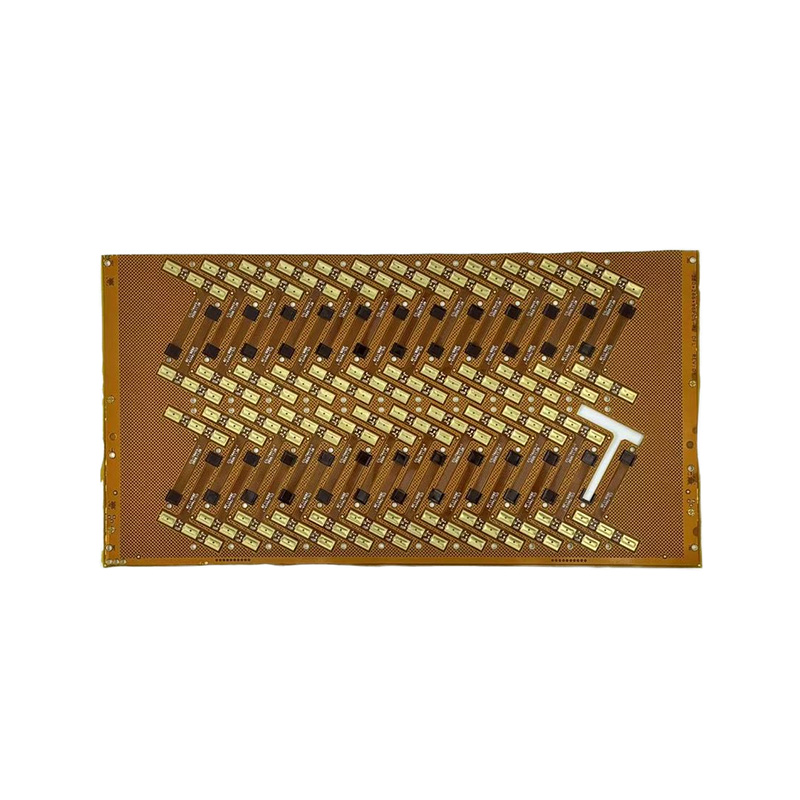
PCB manufacturing — printed circuit board manufacturing — is the industrial process of producing the rigid or flexible boards that mechanically support and electrically connect electronic components in virtually every modern device. From smartphones and laptops to industrial controllers and medical instruments, PCBs are the foundational platform on which electronic systems are built.
A PCB consists of one or more layers of copper conductor traces laminated onto a non-conductive substrate — most commonly FR4 (a glass-reinforced epoxy laminate). The copper traces replace the point-to-point wiring that characterized early electronics, enabling complex circuit topologies to be reproduced reliably and at scale. Modern high-density interconnect (HDI) PCBs may contain 20 or more copper layers in a board just 1.6 mm thick, with trace widths below 75 microns.
Understanding what PCB manufacturing involves — from raw laminate to finished, tested board — matters for engineers, buyers, and product developers who need to make informed decisions about design-for-manufacture, supplier selection, and quality specification.
How a PCB Works: Electrical and Mechanical Fundamentals
Grasping how a PCB works requires understanding the interaction between its three functional elements: the conductive layer, the dielectric substrate, and the component mounting structures.
Copper Trace Conductors
Electrical current flows between components through copper traces etched into each layer of the board. Trace width and thickness determine current-carrying capacity — a 0.5 mm wide, 35 µm thick copper trace can carry roughly 1A continuously without excessive heating under standard conditions. Signal integrity in high-speed designs depends on controlled impedance: the relationship between trace width, dielectric thickness, and the substrate's dielectric constant (Dk), which must be precisely managed to prevent signal reflection and crosstalk in RF and high-frequency digital circuits.
Dielectric Substrate
The insulating substrate separates copper layers and provides mechanical rigidity. FR4 — with a dielectric constant of approximately 4.2–4.5 and a glass transition temperature (Tg) of 130–170°C — is the industry standard for general-purpose PCBs. High-frequency applications use low-Dk materials such as Rogers 4003C (Dk 3.55) or PTFE-based laminates to minimize signal loss at microwave frequencies.
Vias and Layer Interconnection
Vias are plated through-holes or blind/buried holes that connect copper traces across different layers. Through-hole vias span the entire board thickness; blind vias connect an outer layer to one or more inner layers without penetrating to the opposite surface; buried vias connect inner layers only. Via selection directly affects routing density and signal performance in multilayer designs.
Solder Mask and Silkscreen
A polymer solder mask layer — typically green, but available in blue, red, black, and white — covers the copper traces to prevent oxidation and solder bridging during assembly. Silkscreen (legend) ink printed on top provides component reference designators, polarity markers, and manufacturer information for assembly and field service use.
How Are PCB Boards Made: The Step-by-Step Fabrication Process
Understanding how PCB boards are made clarifies why certain design decisions affect cost and lead time. The standard fabrication sequence for a multilayer FR4 board proceeds as follows:
Step 1 — Inner Layer Imaging
Inner copper layers begin as copper-clad laminate panels. A photosensitive dry film resist is laminated onto the copper surface, then exposed to UV light through a photomask (Gerber-generated film or direct laser imaging). The unexposed resist is chemically developed away, and the exposed copper is etched in an alkaline solution, leaving only the desired trace pattern. Trace accuracy at this stage is critical: inner layer registration errors compound across layers in multilayer stackups.
Step 2 — Oxide Treatment and Lamination
Inner layer panels are chemically treated with brown or black oxide to improve adhesion, then interleaved with prepreg (pre-impregnated glass fabric with partially cured resin) sheets and pressed together under heat and pressure — typically 170–185°C at 200–350 psi — in a lamination press. This bonds all layers into a single rigid panel and cures the prepreg resin fully.
Step 3 — Drilling
CNC drilling machines bore through-holes at precise X/Y coordinates for vias and component leads. Drill diameters range from 6.0 mm down to 0.1 mm for microvias. Drilling speed, chip load, and bit wear are tightly controlled to prevent drill wander, smearing of the dielectric into the hole walls, or delamination at the hole exit point.
Step 4 — Desmear and Electroless Copper Plating
Drilling generates resin smear on the hole walls that would block electrical continuity. A plasma or chemical permanganate desmear process removes this contamination. Electroless (autocatalytic) copper deposition then applies a thin seed copper layer — typically 0.5–1.5 µm — to the hole walls and panel surface, providing conductivity for subsequent electroplating.
Step 5 — Outer Layer Imaging and Plating
Outer layers undergo the same imaging process as inner layers, but with an additive approach: resist is applied, exposed, and developed to leave copper areas exposed for plating. Electrolytic copper plating builds the trace and via wall copper to the specified thickness (typically 25–35 µm minimum in hole walls per IPC-6012 Class 2). Tin plating over the copper acts as an etch resist during subsequent outer layer etching.
Step 6 — Etching, Solder Mask, and Surface Finish
Outer layer copper is etched, the tin resist stripped, and solder mask applied by screen or inkjet printing and UV cured. Surface finish is then applied to exposed copper pads: common options include HASL (hot air solder leveling), ENIG (electroless nickel immersion gold), OSP (organic solderability preservative), and immersion silver — each with distinct trade-offs in cost, solderability shelf life, and suitability for fine-pitch components.
Step 7 — Routing, Testing, and Inspection
Panels are routed to individual board outlines by CNC router or scoring. Electrical testing (flying probe or bed-of-nails fixture) verifies every net for opens and shorts. Automated optical inspection (AOI) checks trace geometry, and boards may undergo cross-section analysis or microsection inspection for controlled impedance and via plating thickness verification before shipment.
PCB Production and Assembly: From Bare Board to Functional Unit
PCB production and assembly encompasses both the fabrication of the bare board and the subsequent population of electronic components — a process that transforms an etched laminate into a working electronic assembly. Assembly typically follows one or both of two component mounting technologies:
Surface Mount Technology (SMT)
SMT components — resistors, capacitors, ICs, connectors — are placed directly onto solder paste-printed pads on the board surface by pick-and-place machines at speeds of 20,000–60,000 components per hour for modern high-speed lines. Assembled boards pass through a reflow oven (peak temperature typically 245–260°C for lead-free solder) where the paste melts and forms permanent solder joints. SMT enables dense component placement on both board surfaces and is the dominant technology for consumer and high-volume electronics.
Through-Hole Technology (THT)
Through-hole components — connectors, electrolytic capacitors, transformers, power devices — have leads inserted through drilled holes and soldered on the opposite side by wave soldering or selective soldering machines. THT joints offer higher mechanical pull strength than SMT pads, making them preferred for components subject to mechanical stress or vibration in automotive, industrial, and military applications.
Mixed Technology Assembly
Most contemporary electronic assemblies combine SMT and THT components on the same board. Process sequencing — SMT first or THT first — depends on component placement density, board orientation, and solder process compatibility. Mixed-technology boards require careful thermal profiling to ensure reflow and wave solder processes do not damage previously soldered components.
PCB Fab and Assembly: Understanding the Supply Chain Options
The term PCB fab and assembly — sometimes written as PCBA (printed circuit board assembly) — refers to sourcing both bare board fabrication and component assembly from a single supplier or coordinated supply chain. The choice between integrated and split sourcing has significant implications for quality control, lead time, and cost:
| Sourcing Model | Description | Best Suited For |
|---|---|---|
| Integrated Fab + Assembly (Turnkey) | Single supplier handles bare board fabrication, component procurement, and assembly | New product development, low-to-mid volume, BOM management outsourcing |
| Consigned Assembly | Buyer supplies components; CM handles board fab and assembly only | Buyers with established component supply chains or proprietary sourcing |
| Split Sourcing (Fab + EMS) | Separate suppliers for bare boards and assembly | High-volume production where specialized fab and EMS capabilities are required |
| Prototype + Production Split | Fast-turn prototype fab house; volume production at dedicated assembly plant | Development-stage products transitioning to series production |
Turnkey PCB fab and assembly services reduce the administrative burden of multi-supplier coordination and are particularly valuable for startups and product teams without dedicated supply chain resources. However, buyers should verify that turnkey suppliers maintain full traceability for all components — including certificates of conformance and country-of-origin documentation — to manage counterfeit component risk, which remains a significant issue in contract electronics manufacturing.
How to Use a PCB: Integration, Testing, and Field Considerations
For product developers and system integrators, knowing how to use a PCB correctly — beyond basic electrical connection — determines whether the board performs to specification in the end application. Several practical factors govern successful PCB integration:
Handling and ESD Protection
Bare and assembled PCBs are sensitive to electrostatic discharge (ESD). Handling must follow ANSI/ESD S20.20 protocols: grounded wrist straps, ESD-safe work surfaces, and antistatic packaging for storage and transport. A single ESD event of 500V or more can cause latent damage to MOSFET gate oxides or ESD-sensitive ICs that may not manifest as immediate failure but degrades long-term reliability.
Mounting and Mechanical Stress
PCBs should be mounted using the designed standoff hole pattern to prevent board flexure under vibration or thermal cycling. Excessive board flex — particularly in assemblies where large ceramic capacitors are placed near board edges — can cause component cracking (MLCC fracture) that creates intermittent open or short circuits. For vibration-intensive applications, conformal coating and potting compounds provide additional mechanical protection.
Thermal Management
Heat-generating components — power regulators, processors, RF amplifiers — must be evaluated for junction-to-ambient thermal resistance in the actual mounting environment. Copper pours, thermal vias (arrays of small vias under power pads to transfer heat to inner copper layers or heatsinks), and forced airflow are common thermal management techniques. Failure to manage component temperatures shortens MTBF and may cause immediate thermal shutdown in poorly designed designs.
Incoming Inspection and Functional Test
Before integrating PCBAs into end products, incoming inspection should verify: board dimensions and hole registration, solder joint quality per IPC-A-610 Class 2 or 3 criteria, and functional test results against the test specification. First-article inspection (FAI) on initial production lots catches process drift early, before non-conforming assemblies reach volume production or customer delivery.
Recommended Products

 LET'S CREATE THE FUTURE TOGETHER

Contact Us Anytime
Copyright © Anhui Hongxin Electronic Technology Co., Ltd. All Rights
Reserved.
privacy
Wholesale Printed Circuit Board Suppliers, Manufacturers

