


 English
  Español
  Français
What Is PCB Layout & Design? How to Read and Make a PCB Guide
PCB layout is the process of placing components and routing traces on a board to physically realize a schematic, while PCB design encompasses the complete workflow from concept and component selection to generating manufacturing files. Reading a PCB involves decoding reference designators, polarity marks, and trace patterns, and making a PCB can be achieved through DIY etching or professional fabrication. Getting these fundamentals right matters: even a single layout oversight—like a poorly placed decoupling capacitor—can cause intermittent failures that cost over $10,000 in debugging and re-spins for a medium-complexity board.
What Is PCB Layout and What Is PCB Design?
PCB design is the entire engineering process that transforms a product requirement into a finished board. It starts with component selection and schematic capture, continues through stackup definition and floorplanning, and ends with generating Gerber files and assembly drawings. PCB layout is the central, most time-intensive phase within this process—it is where the designer physically places footprints on the board outline and draws copper traces to create electrical connections. In a typical design cycle, layout work alone can consume 40–50% of the total project time.
The distinction matters because design decisions made before layout directly constrain what is possible. For example, choosing an improper stackup with too-thin dielectric between power and ground layers can raise loop inductance beyond acceptable limits, making it impossible to meet ripple targets regardless of how carefully the traces are routed. Studies on signal integrity show that a poorly planned stackup can increase power distribution network impedance by a factor of five, leading to excessive voltage droop during fast load transients.
Modern PCB design relies heavily on design rule checks (DRCs). Setting accurate constraints for clearances, trace widths, and via sizes before layout begins can catch over 70% of potential manufacturing defects early, according to data from contract manufacturers. This reduces prototype iterations and shortens time-to-market significantly.
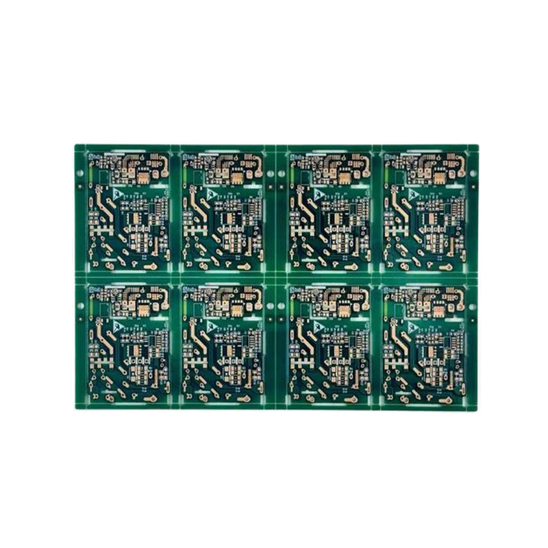
How to Read a PCB Board
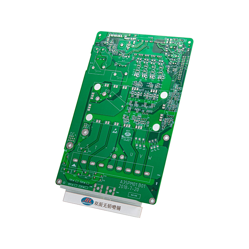
Reading a PCB means interpreting the physical features on the board to understand its function. The most accessible information is on the silkscreen layer—the white text and outlines printed on the board surface.
| Marking | Meaning |
|---|---|
| R5, R12, R101 | Resistors; number matches schematic reference |
| C3, C24 | Capacitors |
| U1, IC2 | Integrated circuits or microchips |
| D2, LED1 | Diodes or LEDs; polarity shown by a flat side or cathode mark |
| TP1, TP_GND | Test points; used to probe signals or voltage rails |
| Pin 1 indicator (dot or notch) | Denotes pin 1 orientation for ICs and connectors |
Beyond the silkscreen, trace width provides hints about current-carrying capacity. On a standard 1 oz copper board, a trace 0.25 mm (10 mils) wide can safely carry about 1 A for a 10°C temperature rise, while a trace 1.0 mm wide handles approximately 2.5 A under the same conditions. Isolated copper fills tied to a net usually serve as heat sinks or shield areas. To fully read a board, you cross-reference these visual clues with a multimeter in continuity mode to map which pins connect—this technique alone can reverse-engineer the netlist of a simple two-layer board in under an hour.
For multi-layer boards, inner layers are invisible, but you can still identify ground and power planes by probing known reference points and observing that many component pins connect to the same low-resistance node. An experienced engineer can estimate the layer count by looking at the board edge under a microscope, counting the dark lines of prepreg between copper foils.
How to Make a PCB: DIY and Factory Methods
Making a PCB can be approached at home for simple prototypes or scaled to professional fabrication for complex, high-reliability boards. Both routes follow the same core sequence: design transfer, patterning, etching, and finishing, but the precision and materials differ radically.
| Aspect | DIY (Home Etching) | Factory Fabrication |
|---|---|---|
| Minimum trace/space | ~0.2 mm (8 mils) | 0.075 mm (3 mils) or finer |
| Layer count | Usually 1 or 2 | Up to 40+ layers |
| Through-hole plating | Rare; often use rivets or wire | Standard, with controlled hole-wall copper |
| Solder mask and silkscreen | Optional; dry film or manual paint | Photoimageable mask, precise silkscreen |
| Typical turnaround | 1–2 hours | 1–5 days (standard) |
| Cost for a 100×100 mm board | Under $5 in materials | ~$0.50–$2 per board in volume |
The DIY route typically uses the toner transfer or photoresist method. In toner transfer, a laser-printed circuit image is ironed onto a copper-clad board, then the board is immersed in ferric chloride or sodium persulfate to dissolve unprotected copper. Drilling is done with a small benchtop drill press. The entire process, from print to a soldered prototype, can be completed in under two hours—a speed advantage that still makes it valuable for rapid, low-frequency proof-of-concept builds.
Factory fabrication, by contrast, achieves far higher precision through photolithography and chemical processes. After imaging dry film resist and etching inner layers, sheets are laminated under heat and pressure to form a multilayer stackup. Computer-controlled drilling creates vias with 0.15 mm diameter or smaller, and electroless copper deposition followed by electrolytic plating coats the hole walls. The final steps add solder mask, surface finish—commonly ENIG (electroless nickel immersion gold) with a gold thickness of 0.05–0.1 µm over 3–6 µm nickel—and silkscreen. Automated optical inspection (AOI) then compares every board to the original Gerber data, catching opens and shorts with 99.5% detection accuracy on modern lines. For high-reliability applications like aerospace, the IPC-6012 Class 3 standard requires a minimum of 25 µm average copper in via barrels, a tolerance home fabrication cannot guarantee.
Whether you etch at home or order from a fab house, the design files you supply are identical: Gerber files and an NC drill file. A free tool like KiCad or a commercial platform like Altium Designer can generate these. A simple LED blinker PCB demonstrates the learning curve: a first-time maker can design and etch a functioning 555 timer board in a weekend, learning to avoid typical errors like acute-angle traces and missing annular rings. That hands-on understanding, in turn, makes you a better designer even when you later outsource fabrication of complex 6-layer high-speed boards.

 LET'S CREATE THE FUTURE TOGETHER

Contact Us Anytime
Copyright © Anhui Hongxin Electronic Technology Co., Ltd. All Rights
Reserved.
privacy
Wholesale Printed Circuit Board Suppliers, Manufacturers

