


 English
  Español
  Français
Single Sided PCB Guide: How It's Made, Advantages & Applications
Content
- 1 What Is a Single Sided PCB
- 2 How Single Sided PCBs Are Made: The Fabrication Process
- 3 Single Sided PCB vs. Double Sided PCB
- 4 Advantages and Cost Profile
- 5 Materials, Applications, and Surface Finishes
- 6 Single Sided PCB Assembly Considerations
- 7 Choosing a 1 Layer PCB Manufacturer for Prototyping and Production
What Is a Single Sided PCB
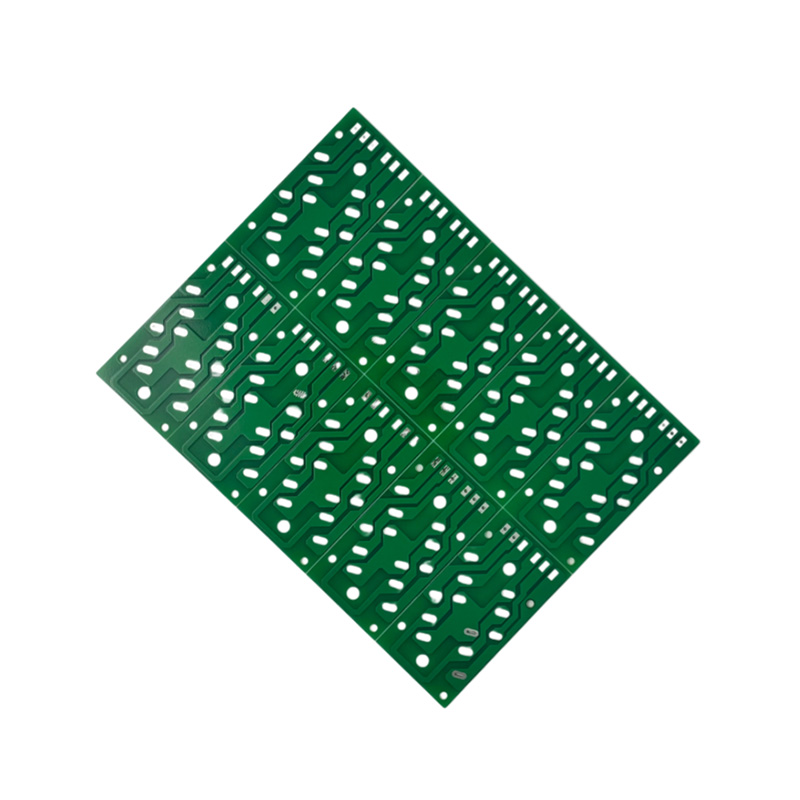
A single sided PCB is a printed circuit board with conductive copper traces on only one side of the substrate, while components are mounted on that same copper side or, in some designs, on the opposite bare side of the board. It's the simplest structural category of PCB, and that simplicity is exactly why it remains widely used decades after multilayer boards became common — fewer manufacturing steps translate directly into lower cost and faster turnaround.
Electrically, a single sided PCB has real limitations compared to double-sided or multilayer boards: with only one copper layer, traces can't cross over each other without a jumper wire or component lead bridging the gap, which caps how dense or complex a circuit can be. That trade-off is generally acceptable for circuits that don't need dense routing in the first place, which is why single-layer boards remain the default choice for a large share of simple, high-volume electronic products.
How Single Sided PCBs Are Made: The Fabrication Process
The single sided PCB manufacturing process follows a shorter version of the same core steps used for any PCB, with fewer layers to align and laminate:
- Substrate preparation — a copper-clad laminate sheet (FR-4, FR-1, CEM-1, or another base material) is cut to panel size and cleaned.
- Circuit imaging — the trace pattern is transferred onto the copper layer using photoresist and UV exposure, defining exactly which copper should remain and which should be etched away.
- Etching — chemical etching removes all unwanted copper, leaving only the traces defined by the imaged pattern.
- Drilling — holes for through-hole components and mounting points are drilled at this stage, since there's no internal layer alignment to account for.
- Solder mask application — a protective coating is applied over the copper traces, leaving only pads and connection points exposed.
- Surface finish — a final coating is applied to exposed copper pads to protect against oxidation and improve solderability.
- Silkscreen and electrical testing — component labels are printed, and the finished board is electrically tested before shipment.
Because there's no layer-to-layer registration to manage, this is why how are single sided PCBs made tends to come with noticeably shorter lead times than multilayer equivalents — fewer process steps mean fewer opportunities for defects and less total production time per panel run.
Single Sided PCB vs. Double Sided PCB
The comparison between single sided PCB vs double sided PCB — sometimes phrased as single layer PCB vs double layer PCB — comes down to a routing density and cost trade-off:
| Factor | Single Sided PCB | Double Sided PCB |
|---|---|---|
| Copper layers | 1 | 2, connected by plated through-holes |
| Routing density | Limited; no trace crossovers without jumpers | Higher; traces can cross using both layers |
| Unit cost | Lowest | Moderately higher |
| Typical use case | Simple, high-volume, cost-sensitive circuits | Moderately complex circuits needing denser routing |
The decision usually isn't about which board is "better" in the abstract — it's about whether the circuit's complexity genuinely needs the extra routing layer. Specifying a double-sided board for a circuit that would fit comfortably on one layer adds cost and lead time without a functional benefit.
Advantages and Cost Profile
The main single sided PCB advantages all trace back to the same root cause — fewer layers and simpler processing:
- Lower per-unit cost — fewer materials and process steps make single sided boards the most economical PCB category for a given board size.
- Faster production and prototyping turnaround — no layer alignment or lamination steps means shorter cycle times per batch.
- Simpler quality control — with only one copper layer to inspect and test, defect detection and rework are more straightforward than on multilayer boards.
- Easier rework and repair — components and traces are fully accessible from one side, simplifying field repairs or design revisions.
This combination is exactly why low cost PCB manufacturing programs — especially for consumer products competing heavily on price — default to single-layer designs wherever the circuit complexity allows it, reserving multilayer boards for the subset of products that genuinely need the extra routing capacity.
Materials, Applications, and Surface Finishes
FR4 single sided PCB boards are the most common choice where mechanical strength and good insulation matter, while lower-cost materials like FR-1 or CEM-1 suit simpler, less demanding applications where the extra durability of FR-4 isn't necessary. Metal-core substrates are used instead of standard laminate when heat dissipation is the priority, particularly for high-power LED applications.
| Application Area | Typical Products |
|---|---|
| Consumer electronics | Power adapters, chargers, LED drivers |
| Home appliances | Washing machines, microwave ovens, air conditioners |
| Industrial control | Power control boards, relay modules |
| Lighting | LED lighting boards, street light controllers |
Single sided PCB surface finish options each suit different priorities: HASL is cost-effective with strong solderability for general products; lead-free HASL meets RoHS requirements for export markets; ENIG offers a flatter surface with longer shelf life for fine-pitch components; and OSP is a low-cost, environmentally friendly option common in high-volume production runs.
Single Sided PCB Assembly Considerations
Single sided PCB assembly is generally more straightforward than assembling multilayer boards, since all components and solder joints sit on one accessible side. Through-hole components are typically inserted from the bare (non-copper) side and soldered on the copper side, while surface-mount components are placed and reflowed directly on the copper side alongside the trace pattern.
Wave soldering remains a common assembly method for single sided boards with through-hole components, since the board's single accessible solder side suits the wave soldering process well — the board passes over a wave of molten solder that only needs to contact one side, rather than requiring the more complex handling needed for double-sided reflow assembly.
Choosing a 1 Layer PCB Manufacturer for Prototyping and Production
Not every 1 layer PCB manufacturer handles prototype and bulk orders with the same turnaround, and lead time consistency matters more for single sided boards than the underlying technology might suggest — since these boards are so often used in high-volume, cost-sensitive products, a supplier's ability to hold delivery schedules across large production runs is often more important than any single technical specification.
For buyers evaluating a prototype single sided PCB run before committing to volume production, Anhui Hongxin Electronic Technology Co., Ltd. is worth considering — the company operates a 20,000-square-meter facility in Anhui's PCB Industrial Park with ISO9001, ISO14001, ISO45001, and IATF16949 certification, and typically delivers single- and double-sided bulk orders within 6-7 days alongside fast prototyping turnaround, which suits both early-stage design validation and larger production commitments without switching suppliers between the two stages.

 LET'S CREATE THE FUTURE TOGETHER

Contact Us Anytime
Copyright © Anhui Hongxin Electronic Technology Co., Ltd. All Rights
Reserved.
privacy
Wholesale Printed Circuit Board Suppliers, Manufacturers

