

 English
  Español
  Français
How to Design and Fix a PCB Board: A Complete Beginner's Guide
Content
What Is a PCB and Why Design Matters
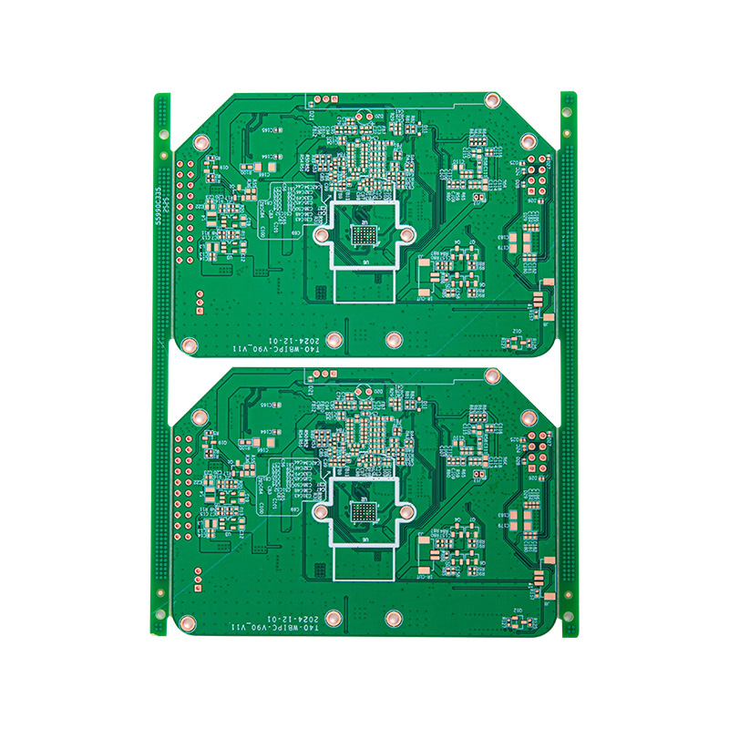
A printed circuit board (PCB) is the physical foundation of nearly every electronic device — from smartphones to industrial controllers. It mechanically supports and electrically connects components using conductive copper tracks etched onto a non-conductive substrate, most commonly FR4 fiberglass. Getting the design right from the start determines not just whether a circuit works, but whether it will be manufacturable, reliable, and cost-effective at scale.
PCB design is distinct from schematic design. A schematic defines the logical connections between components; a PCB layout translates those connections into physical geometry — trace widths, layer stackups, component placement, and drill holes. Errors at the layout stage can cause signal integrity problems, excessive electromagnetic interference (EMI), thermal failures, or outright shorts that a perfect schematic would never predict.
How to Design a PCB: The Step-by-Step Process
The PCB design workflow follows a consistent sequence regardless of the software used. Understanding each stage prevents rework and reduces manufacturing defects.
Step 1 — Draw the Schematic
Before placing a single component on a PCB canvas, the schematic must be complete and error-free. Use EDA (Electronic Design Automation) software such as KiCad (free), Altium Designer, Eagle, or EasyEDA to draw all components, assign reference designators, and run an Electrical Rules Check (ERC). Any unresolved ERC warning at this stage will propagate into the layout.
Step 2 — Define the Board Outline and Layer Stackup
Set the board dimensions in the PCB editor. For beginners, a 2-layer board (top copper + bottom copper) is sufficient for most hobby and low-frequency commercial projects. High-speed digital or RF designs may require 4 or more layers to provide dedicated ground and power planes that control impedance. Specify material, finished board thickness (commonly 1.6 mm), and copper weight (typically 1 oz/ft²).
Step 3 — Place Components Strategically
Import the netlist from the schematic and begin placing components. Follow these placement principles:
- Place connectors and mounting holes first to anchor the board's mechanical constraints.
- Group components by function — keep power regulation, analog, and digital sections physically separated to reduce noise coupling.
- Position decoupling capacitors as close as possible to IC power pins — ideally within 0.5 mm.
- Orient components to minimize trace crossings, which reduces the number of vias needed.
Step 4 — Route Traces
Routing converts the ratsnest (unrouted connections shown as straight lines) into physical copper traces. Key rules to follow:
- Trace width must be sized for the current it carries. A 0.25 mm trace handles roughly 0.5 A in typical conditions; a 1 mm trace can handle approximately 2 A. Use an online trace width calculator for precision.
- Power and ground traces should be wider than signal traces — 0.5–1 mm minimum for low-power boards.
- Avoid 90° corners in traces; use 45° angles or curves to prevent acid traps during etching and to reduce impedance discontinuities at high frequencies.
- Use a copper pour (ground fill) on unused board areas to create a solid ground reference plane.
Step 5 — Run Design Rule Check (DRC) and Generate Gerbers
Run the DRC tool to catch minimum clearance violations, unconnected nets, or silkscreen overlaps. Once the board passes, export Gerber files (one per layer) and a drill file. These files are what PCB fabricators use to manufacture your board. Most manufacturers — JLCPCB, PCBWay, OSH Park — accept standard Gerber RS-274X format.
How to Create a PCB Board: Fabrication Options
Once design files are ready, there are two practical paths to a physical board: professional fabrication or DIY etching.
| Method | Minimum Trace Width | Turnaround | Best For |
|---|---|---|---|
| Professional fab (e.g., JLCPCB) | 0.1 mm (4 mil) | 2–7 days | All projects, highest quality |
| DIY toner transfer + etching | 0.5–1 mm | 1–2 hours | Prototyping, single-layer boards |
| CNC milling (PCB router) | 0.3–0.5 mm | 30–90 minutes | In-house rapid iteration |
For beginners, ordering from a professional PCB fabricator is strongly recommended. Five 2-layer boards of 100 × 100 mm typically cost under $5 USD from budget services, with no minimum order quantity requirement. The quality advantage — solder mask, silkscreen, HASL or ENIG finish — is impossible to replicate with DIY methods at that price point.
How to Fix a PCB Board: Diagnosing and Repairing Common Faults
PCB repair is a systematic process of fault isolation before physical intervention. Attempting component replacement without first identifying the root cause wastes parts and risks further damage.
Visual Inspection First
Under magnification (10× loupe or digital microscope), look for: burnt components (discoloration, cracked casings), cold solder joints (dull, grainy, or cracked fillets), solder bridges (unintended shorts between adjacent pads), and lifted pads (copper pad delaminated from the substrate). Many faults are visible before any electrical testing.
Electrical Fault Isolation
Use a digital multimeter (DMM) in continuity mode to check suspected short circuits between power and ground. In resistance mode, compare readings against the schematic. An in-circuit ESR meter is invaluable for testing electrolytic capacitors without desoldering — a capacitor with ESR above 1–5 Ω (depending on rating) is typically failing and will cause power supply instability or ripple-related failures.
Common Repairs and Techniques
- Resoldering a cold joint: Apply fresh flux, touch the soldering iron tip to the joint for 2–3 seconds, then add a small amount of 63/37 tin-lead or SAC305 lead-free solder. The fillet should be smooth and shiny.
- Removing a solder bridge: Apply flux, then drag a clean iron tip across the bridge. If it persists, use copper desoldering braid (wick) pressed firmly against the bridge with the iron tip on top.
- Repairing a broken trace: Scrape back the solder mask 5–10 mm on both sides of the break, tin the exposed copper, and bridge the gap with a length of 30 AWG wire-wrap wire or solder. Secure with a dot of UV-cure PCB repair lacquer.
- Replacing a damaged through-hole component: Use a desoldering pump or wick to remove old solder, lift the component, clean the holes with a 0.8 mm drill bit if clogged, insert the replacement, and solder from the opposite side.
- Replacing SMD components: For small passives (0402, 0603), use fine-tip tweezers and a soldering iron with a 1–2 mm chisel tip. For ICs with many pins, hot air rework is faster — apply flux, set the rework station to 320–360 °C (adjust for lead-free), and move the nozzle in a circular pattern until the part lifts freely.
Post-Repair Verification
After any repair, clean the board with isopropyl alcohol (IPA 99%) and an ESD-safe brush to remove flux residue, which can be mildly corrosive over time and can cause leakage currents in high-impedance circuits. Re-test continuity at repaired nodes before applying power. For boards that have experienced a power fault, use a bench power supply with adjustable current limiting — set the limit to 10–20% of the normal operating current and raise voltage slowly while monitoring for unexpected current draw.
PCB Design Tips for Beginners: Mistakes to Avoid
Most beginner PCB failures stem from a small set of recurring errors. Awareness of these patterns significantly reduces first-spin success rates:
- Wrong footprint: Always verify component footprints against the physical datasheet dimensions before ordering. A 0805 capacitor footprint will not accept a 1206 package. Cross-check land pattern dimensions — pad size, pitch, and courtyard — against the manufacturer's recommended land pattern, not just the component body dimensions.
- Ignoring thermal relief: Large copper pours connected directly to through-hole component pads make soldering extremely difficult. Use thermal relief spokes (typically 4 connections, 0.3–0.5 mm wide) between the pad and the pour to allow the pad to reach soldering temperature quickly.
- Insufficient clearance around mounting holes: Allow at least 3 mm of keep-out zone around mounting holes if using metal standoffs, to prevent screws from shorting exposed traces or vias.
- No test points: Add exposed copper test pads to key nodes — power rails, ground, and critical signals — before sending to fab. They cost nothing in manufacturing and save hours during debugging.
- Skipping the review checklist: Before generating Gerbers, run through a standard checklist: all components placed, all nets routed, DRC clean, board outline closed, drill file included, layer assignments correct. A 10-minute review prevents a 2-week re-spin cycle.
One practical benchmark: Professional PCB designers target a first-spin success rate above 90%. Beginners commonly achieve 50–60% on the first attempt — not because of complex errors, but because of avoidable footprint and clearance mistakes that a structured review process would catch.


 LET'S CREATE THE FUTURE TOGETHER

Contact Us Anytime
Copyright © Anhui Hongxin Electronic Technology Co., Ltd. All Rights
Reserved.
privacy
Wholesale Printed Circuit Board Suppliers, Manufacturers
![]()
