


 English
 Español
 Français

PCB Routing Rules: Trace Width, Spacing, and Manufacturing Choices That Matter
Every routed board we see at our factory tells a story about the decisions made before it arrived. A schematic defines the electrical function, but routing decides whether that function can be manufactured at a sensible cost, within a realistic lead time, and with enough margin to survive years of heat, vibration, and voltage stress. In our experience as a PCB manufacturer, most preventable production problems — burnt traces, failed clearances, warped panels, poor plating — trace back to a handful of routing rules that were either missed or misunderstood. This article explains what routing a PC board really involves, which parameters matter most, and how to set routing constraints that a factory can actually build without dispute.
Content
- 1 What Routing a PC Board Actually Involves
- 2 Trace Width: The First Route Decision
- 3 Clearance and Spacing: Set Them for Voltage, Not Just for the Design Rule Check
- 4 Layer Stackup: Routing Density Drives Cost and Lead Time
- 5 DFM Rules: Route the Way a Factory Etches, Plates, and Laminates
- 6 Materials and Surface Finishes That Change Routing Rules
- 7 Route With Manufacturing in Mind
What Routing a PC Board Actually Involves
Routing is the layout step in which every electrical net in the schematic becomes a physical copper path. Software can draw those paths automatically, but the result is only as good as the constraints the designer provides: trace width, spacing between conductors, allowed layers, via types, and the copper distribution that the etching and plating process will see.
The route also creates the ground reference planes, power islands, and thermal paths that make a design work in the real world. Placing components decides where parts sit; routing decides how they connect. Between the two, routing has the larger influence on manufacturing cost and yield, because trace geometry and copper balance directly affect how the factory etches, plates, and laminates the panel.
Trace Width: The First Route Decision
Trace width is the first number to set because it carries three requirements at once: current capacity, voltage drop, and characteristic impedance. Signal traces can be thin; power nets need cross-section. The reference used by most factories is IPC-2221. For 1 oz (35 µm) copper on an external layer with a 10°C temperature rise, the estimated current capacity is roughly as follows.
| Trace width (mil) | Trace width (mm) | Max current (A) |
|---|---|---|
| 10 | 0.25 | 0.9 |
| 20 | 0.50 | 1.5 |
| 40 | 1.00 | 2.4 |
| 60 | 1.50 | 3.2 |
| 100 | 2.50 | 4.7 |
Two corrections matter in practice. Traces on internal layers dissipate roughly half as much heat as external traces, so the current table should be derated accordingly. And these values assume a modest 10°C rise; if the surrounding enclosure blocks airflow or the ambient temperature is high, the safe current drops further. When a design must carry sustained high current, the route should use a copper pour, a plane, or a thicker copper layer rather than a single narrow trace. Our line regularly routes 2 oz to 10 oz thick copper boards, and the trace width tables for those weights look very different from the 1 oz values above.
Clearance and Spacing: Set Them for Voltage, Not Just for the Design Rule Check
Clearance is the distance between two copper features: trace to trace, trace to pad, pad to via. A design rule check will verify whatever number is typed into the CAD tool, but the right number comes from voltage, signal integrity, and factory capability, not from a default rule. For low-voltage signal nets inside an enclosed product, 0.1 mm (4 mil) between traces is common; our standard capability is 4 mil, and we can hold 3 mil trace and space where design density requires it.
Clearance should not be a single global value. Working voltage, pollution degree, coating, altitude, and transient voltages all influence the creepage distance a product needs. IPC-2221B contains the spacing-versus-voltage tables that compliance engineers use; as a practical rule, any net carrying more than 50 V, or any trace routed near the board edge, should use substantially larger clearance than the default design rule.
For high-speed signals, spacing controls both coupling and impedance. A matched differential pair holds its target impedance only when the gap between the two traces remains constant, and the reference plane underneath matters more than the absolute clearance value. For RF circuits, a 50 Ω trace is defined by its width, the dielectric thickness, and the distance to the ground plane below it.
Layer Stackup: Routing Density Drives Cost and Lead Time
The number of layers is the biggest routing decision a design makes. If two layers can handle the density, a six-layer stackup is wasted money. If the design needs continuous power and ground planes, tight impedance control, or dense BGA fan-out, the stackup moves to four, six, or more layers. Moving from two layers to four roughly doubles process cost, because inner-layer imaging, lamination, alignment, and additional drill steps are added to the route. Lead times grow with layer count as well. At our facility in the Guangde Economic Development Zone, published production lead times by layer count are as follows.
| Board type | Standard lead time |
|---|---|
| Single-sided / double-sided batch | 6-7 days |
| 4-8 layers | 9-20 days |
| 10-16 layers | 20-25 days |
| 16-32 layers | 25-45 days |
| HDI boards | Within 25 days |
| Double-sided prototype | 24 hours (fastest) |
The route sets the stackup, and the stackup sets the delivery date. If a design only needs 12 layers because the outer signal layers are poorly used, a cleaner four-layer route would have arrived in a fraction of the time. Our factory builds from 1 to 32 layers, and the pattern is consistent: efficient routing shortens lead time more reliably than any expedite fee.
DFM Rules: Route the Way a Factory Etches, Plates, and Laminates
A route that passes netlist and signal checks can still fail on the factory floor. The board must be etched, drilled, plated, and pressed, and each process has geometric limits. The following rules prevent the most common repeat failures.
Copper Balance and Thieving
When one area of a layer is a solid pour and another is nearly empty, plating thickness becomes uneven and lamination can warp the panel. Good routing distributes copper across every layer; where that is impossible, add thieving blocks or cross-hatched copper. Our CAM team adds thieving during tooling, but a routed design that arrives balanced passes review faster and plates more uniformly.
Vias and Annular Ring
Every via needs an annular ring: the copper ring around the drilled hole that connects the barrel to the trace. If the ring is too small, drill misregistration breaks the connection. A minimum 4 mil (0.1 mm) annular ring is a safe working rule for standard processing. Blind and buried vias reduce layer count in dense designs, but each via type adds drilling and lamination steps; via-in-pad, useful under BGAs, requires filling and additional plating. HDI boards with microvias form a separate process family, which our HDI line delivers within 25 days.
Thermal Reliefs
When a through-hole pad connects to a large copper pour, the pour acts as a heat sink during soldering. Without thermal relief spokes, the pad may not reach soldering temperature. Route plane-connected pads with thermal reliefs wherever the current rating permits.
A practical routing checklist to run before sending files:
- Size power traces and pours for sustained worst-case current, not for the typical load.
- Use per-net-class clearance rules; high-voltage, high-speed, and general signal nets rarely need the same spacing.
- Keep the copper distribution on each layer reasonably even, and add thieving to layers that are mostly empty.
- Confirm the minimum trace/space, minimum annular ring, and minimum via drill size with the factory before finalizing the route.
- Place a solid reference plane under every high-speed or impedance-controlled route.
Materials and Surface Finishes That Change Routing Rules
The substrate and finish change routing parameters as much as the electrical circuit does. Standard FR-4 handles general digital and analog boards well. High-Tg FR-4 resists CAF failure in thick multilayer boards and is common in automotive electronics; halogen-free FR-4 covers environmental requirements; high-frequency laminates with controlled Dk and Df are used for RF and high-speed digital, and the trace width needed for a 50 Ω line changes with each material.
Metal-core boards — aluminum or copper base — conduct heat through the substrate, so power circuits can use narrower routes, but drilling and etching of metal cores follow different design rules. Our product range includes FR-4, high-Tg, halogen-free, high-frequency, aluminum-base, copper-base, and ceramic-based boards, with surface finishes such as OSP, lead-free HASL, immersion gold, and immersion tin. Finish choice mainly affects solderability and shelf life, so it should be matched to the assembly process rather than treated as an afterthought.
Route With Manufacturing in Mind
Routing is where a design becomes a physical object, and that object is judged by a factory. Boards that ship on time and work reliably are rarely the products of clever auto-router settings; they are the products of trace widths sized for current, clearances set for voltage, stackups chosen for density, and DFM details respected from the first layout pass. When in doubt, ask early: a double-sided prototype from our factory can turn in 24 hours, and one fast iteration costs far less than a 16-layer batch that fails electrical test because of a spacing error. If you need a stackup recommendation, a DFM review, or a quote for a routed board from 1 to 32 layers, our engineering team is set up to answer with specifics.
Recommended Products
-
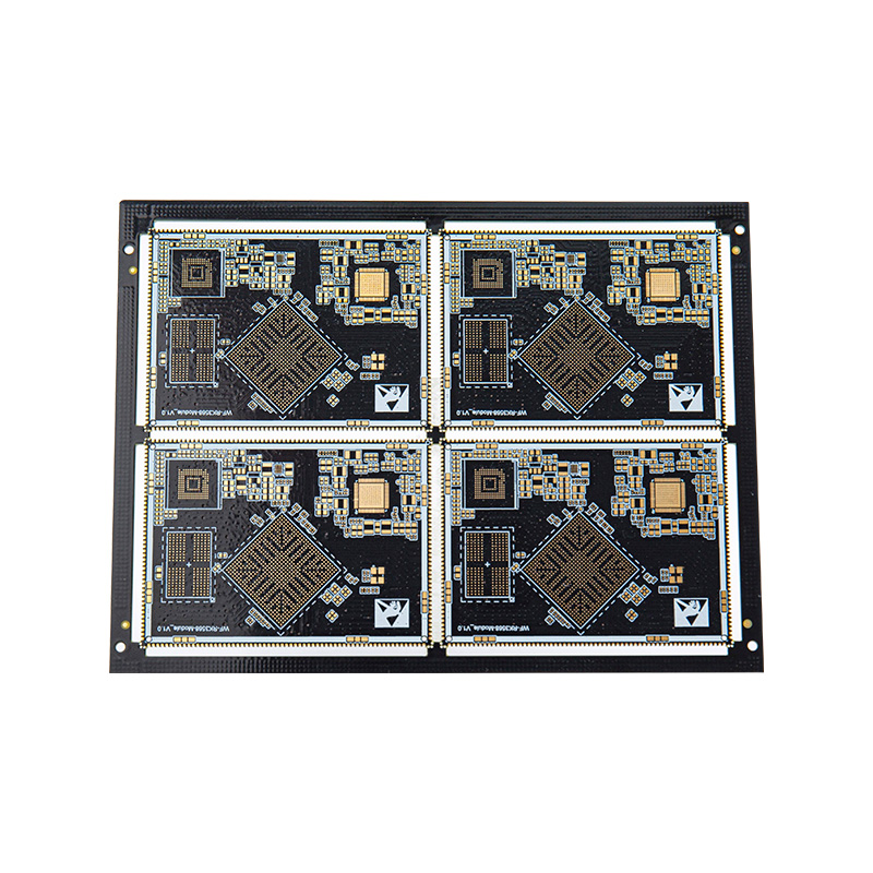

6-Layer Gold-Plated Board, Line Width And Spacing Of 3/3, BGA, Half-Hole Technology
-
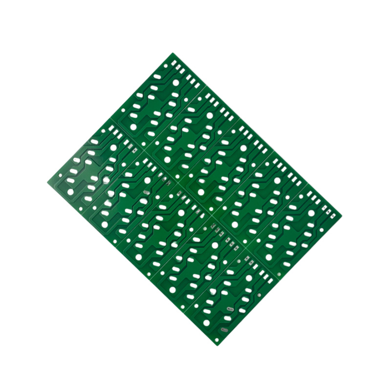
Single-Sided Tin-Spraying PCB Board
-
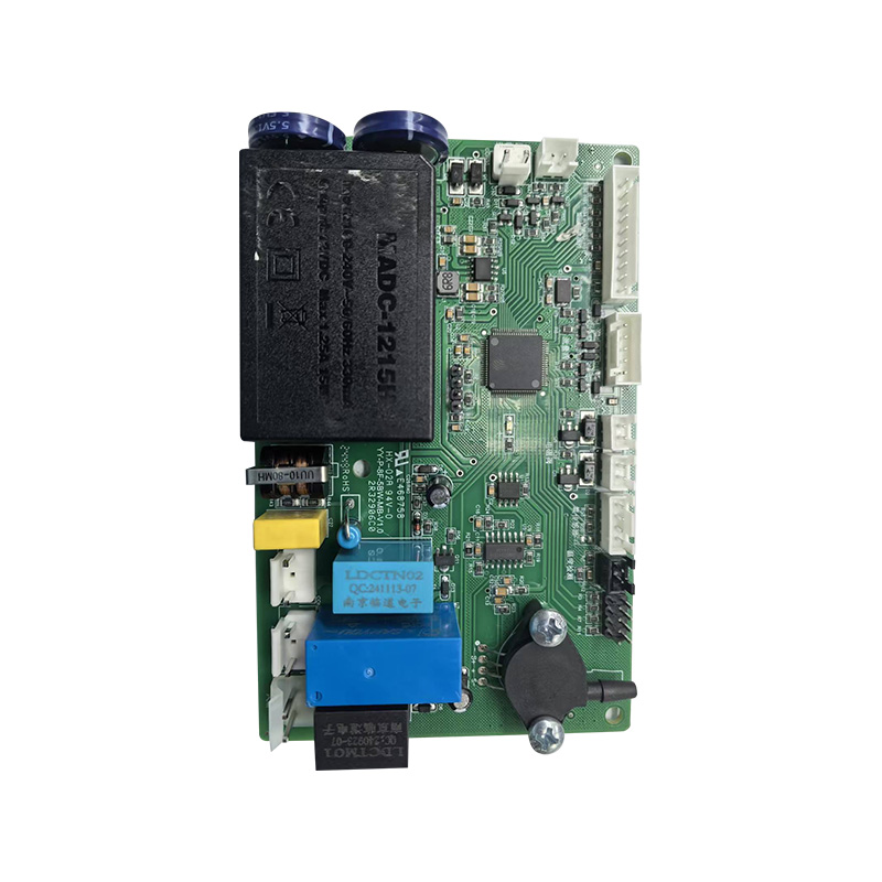
Oxygen Concentrator PCBA
-
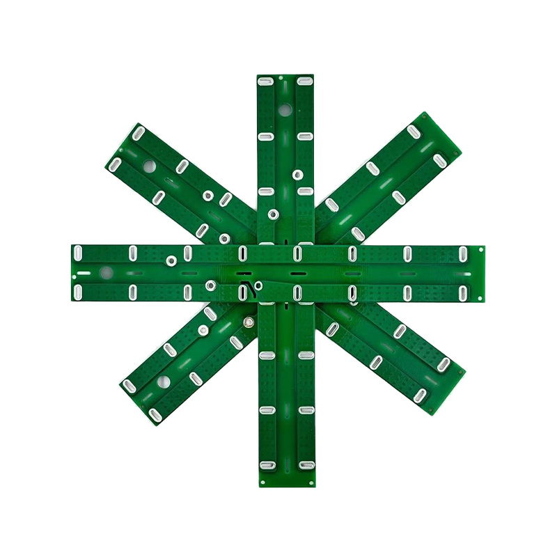
Durable Double-Layer Green Lead-Free PCB
-
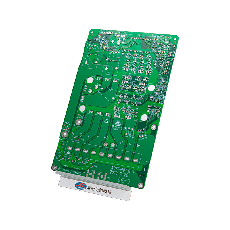
Double-Sided Green Lead-Free Soldered PCB For Power & Automotive Electronics
-
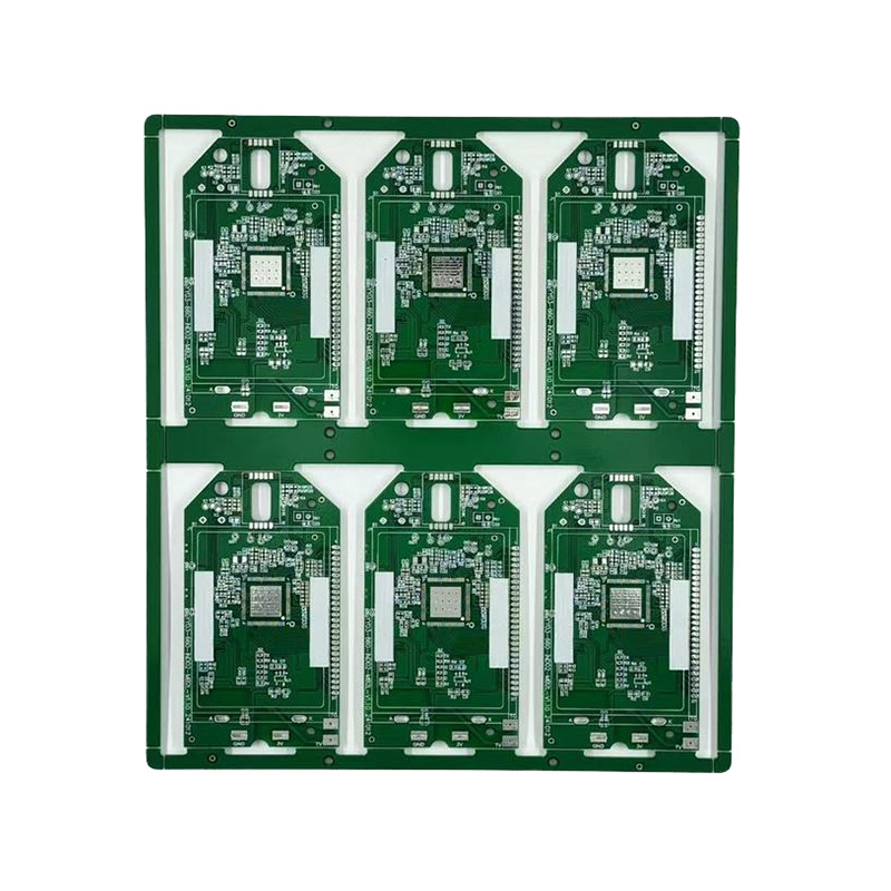
Double-Sided Lead-Free Soldered Green PCB With Enhanced Oxidation Resistance
 LET'S CREATE THE FUTURE TOGETHER

Contact Us Anytime
Copyright © Anhui Hongxin Electronic Technology Co., Ltd. All Rights
Reserved.
privacy
Wholesale Printed Circuit Board Suppliers, Manufacturers

