

 English
  Español
  Français
Quick Turn PCB Fabrication & SMT Assembly: Processes, AI Optimization, and Partner Selection
Content
- 1 Quick Turn PCB Fabrication: What It Is and When It Matters
- 2 PCB Fabrication Specifications That Affect Quick Turn Availability
- 3 Surface Mount Technology PCB: How SMT Defines Modern Electronics Assembly
- 4 Components on a PCB: The Major Categories and Their Assembly Implications
- 5 Artificial Intelligence in PCB Assembly Optimization: Where It Is Being Applied
- 6 Selecting a PCB Fabrication and Assembly Partner: What to Evaluate
Quick Turn PCB Fabrication: What It Is and When It Matters
Quick turn PCB fabrication is the accelerated production of printed circuit boards — typically delivered in 24 hours to 5 business days from Gerber file submission — compared to the 10–15 day standard lead time of conventional production runs. The speed premium exists because prototype and engineering validation cycles are gated by physical hardware availability: a firmware team that receives PCBs five days earlier can complete an iteration cycle in one week that would otherwise take three, compressing a 12-month product development timeline by months rather than days.
Quick turn PCB fabrication is not a separate technology from standard PCB manufacturing — it uses the same photolithographic imaging, copper etching, lamination, drilling, and surface finishing processes. The speed comes from priority scheduling on production lines, pre-staged raw material inventory (standard FR-4 cores, prepregs, copper foils, and soldermasks in the most common specifications), automated DFM checking that clears files for production within minutes of upload, and panel-sharing arrangements that allow low-volume prototype orders to ship alongside other customers' boards on the same production panel without waiting for a dedicated panel to fill.
The trade-off is cost: quick turn pricing carries a 2x–5x premium over standard lead time pricing for equivalent specifications, reflecting the scheduling disruption, inventory carry cost, and reduced panel utilization that expedited orders impose on the fabricator. For prototype quantities of 5–10 boards, this premium is typically USD 50–300 additional cost — negligible relative to the engineering labor cost of a delayed iteration cycle. For production quantities above 500 boards, the calculus changes and the premium is harder to justify except in genuine supply chain emergency situations.
PCB Fabrication Specifications That Affect Quick Turn Availability
Not all PCB designs are equally suited to quick turn production. Certain specifications push boards outside the standard material and process inventory that makes same-day or next-day fabrication possible. Understanding which parameters constrain quick turn availability helps engineers make design decisions that preserve schedule flexibility:
- Layer count: 2-layer and 4-layer boards are the fastest to produce because standard laminate stackups are pre-staged. 6-layer boards are available in quick turn at most major fabricators; 8-layer and above typically add 1–3 days even on expedite schedules due to lamination cycle complexity.
- Minimum trace/space: Designs at 3/3 mil (75 µm) trace and space require high-density imaging equipment not available at all facilities. 4/4 mil (100 µm) and above are producible at virtually any quick turn fabricator. For 3/3 mil or finer, confirm capability before submitting.
- Surface finish: HASL (hot air solder levelling) and ENIG (electroless nickel immersion gold) are stocked at all quick turn facilities. OSP (organic solderability preservative) and ENEPIG are available at most; hard gold, immersion silver, and immersion tin may add lead time at some facilities.
- Controlled impedance: Designs requiring impedance-controlled traces (50 Ω, 90 Ω differential, etc.) need stackup confirmation and coupon testing, which adds 4–8 hours to the production cycle but is compatible with 24–48 hour quick turn at facilities with in-house TDR measurement.
- Special materials: High-Tg FR-4 (Tg ≥170°C), Rogers high-frequency laminates, aluminium-backed IMS boards, and flex or rigid-flex constructions fall outside standard quick turn inventory at most fabricators. Lead times of 5–10 days are typical even on expedite schedules for these material sets.
Surface Mount Technology PCB: How SMT Defines Modern Electronics Assembly
Surface mount technology (SMT) is the dominant PCB assembly method in virtually all contemporary electronics, from consumer devices to industrial controls to aerospace systems. In SMT assembly, components are placed directly onto pads on the PCB surface rather than inserted through holes in the board — the through-hole (THT) approach that preceded SMT and still coexists with it for specific component types.
SMT enables component placement densities and board miniaturization that through-hole assembly cannot approach. A 0402 resistor (1.0 mm × 0.5 mm) occupies approximately 0.5 mm² of board surface; its through-hole equivalent requires a 0.8 mm drill hole plus annular ring on both sides of the board, consuming 3–5× the board area and requiring a hole through every internal layer. At the system level, SMT allows multi-layer boards densely populated on both sides, enabling the compact form factors of smartphones, wearables, and modern computing hardware that would be physically impossible with through-hole construction.
The SMT assembly process sequence is standardized across the industry:
- Solder paste printing: A stencil (laser-cut stainless steel, typically 0.12–0.15 mm thick) is aligned to the bare PCB and a squeegee deposits solder paste through apertures onto the component pads. Paste volume consistency is the single most critical variable in downstream solder joint quality.
- Component placement: Pick-and-place machines position components onto the paste-printed pads. Modern high-speed placement machines achieve placement rates of 20,000–120,000 components per hour at accuracies of ±25–50 µm.
- Reflow soldering: Boards pass through a reflow oven with a carefully profiled temperature curve — typically peaking at 235–250°C for SAC305 lead-free solder — that melts the paste, wets the component terminations, and solidifies to form metallurgical solder joints.
- Inspection: Automated optical inspection (AOI) and, for critical assemblies, automated X-ray inspection (AXI) verify joint quality, component presence and polarity, and paste coverage before boards proceed to test.
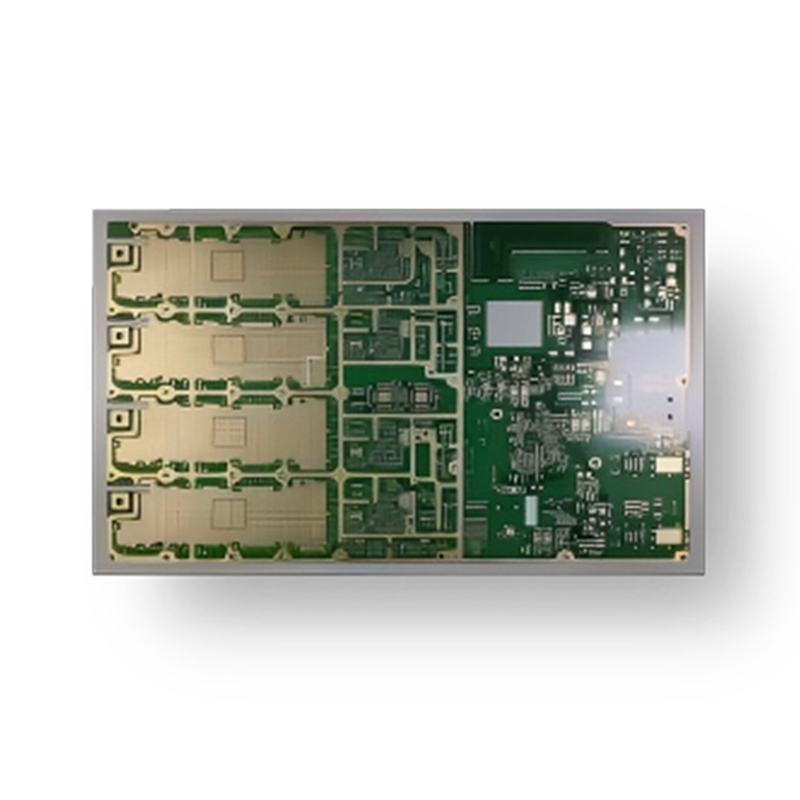
Components on a PCB: The Major Categories and Their Assembly Implications
A populated PCB integrates multiple component categories, each with distinct handling requirements, placement tolerances, and inspection criteria. Understanding the component mix on a board is essential for assembly planning, stencil design, and process optimization.
| Component Category | Common Package Types | Assembly Method | Key Assembly Consideration |
|---|---|---|---|
| Passive components (R, C, L) | 0201, 0402, 0603, 0805, 1206 | SMT reflow | Tombstoning risk on 0201/0402; paste volume balance critical |
| ICs — leaded (gull-wing) | SOIC, QFP, TSSOP | SMT reflow | Lead coplanarity ≤0.1 mm; solder bridging at fine pitch (<0.5 mm) |
| ICs — area array (BGA, LGA) | BGA, µBGA, LGA, QFN | SMT reflow | Hidden joints require X-ray inspection; voiding in thermal pads |
| Connectors | Board-to-board, wire-to-board, USB, RJ45 | SMT or THT wave / selective solder | Mechanical stress relief; pin straightness for THT insertion |
| Power components | TO-220, D2PAK, IPM modules | THT or SMT + clip/screw mount | Thermal interface to heatsink; high current pad design |
| Electromechanical (relays, switches) | DIP relay, SMD relay, tactile switch | THT wave or SMT reflow | Flux contamination ingress; wash compatibility |
Mixed-technology boards — containing both SMT and THT components — require a two-pass assembly process: SMT components are reflowed first, then THT components are inserted and wave-soldered or selectively soldered. The challenge is that wave soldering exposes the underside of the board to a solder wave at 250–260°C, which can re-melt or dislodge SMT components already placed on that side. SMT components on the secondary side of a mixed-technology board must either be adhesive-bonded before wave soldering or restricted to components with mass and pad geometry low enough that surface tension holds them in place during the wave pass.
Artificial Intelligence in PCB Assembly Optimization: Where It Is Being Applied
AI-driven optimization is being integrated into PCB assembly operations across multiple process stages, driven by the convergence of affordable machine vision, edge computing hardware capable of real-time inference, and large proprietary datasets of assembly process outcomes accumulated by high-volume contract manufacturers over decades of production.
The manufacturing intelligence gap that AI addresses is the mismatch between the amount of process data generated by a modern SMT line and the human capacity to act on it. A single high-speed pick-and-place machine generates placement coordinate data, nozzle vacuum pressure readings, component thickness measurements, and fiducial correction vectors for every component on every board — potentially 50,000–120,000 data points per hour. A reflow oven logs thermocouple readings from 10–20 zones at 1-second intervals. An AOI system produces defect images and classification decisions for every joint on every board. The aggregate data rate from a five-machine SMT line is in the range of 100,000–500,000 data points per hour, far beyond the capacity of manual statistical process control to monitor and act on in real time.
Solder Paste Inspection and Print Process Optimization
3D solder paste inspection (SPI) systems equipped with AI classification models have moved beyond simple pass/fail volume checking to predictive process control: the AI correlates current paste deposit volume, shape, and offset data with historical reflow defect outcomes to predict which boards are at elevated risk of bridging or opens before they enter the oven, enabling the operator to clean and re-print a specific board rather than discovering the defect after reflow. Some systems automatically adjust stencil printer parameters — squeegee speed, pressure, separation speed — in closed-loop response to SPI measurements without operator intervention, maintaining print quality as stencil apertures wear and paste rheology drifts through a production shift.
Placement Machine Optimization and Predictive Maintenance
AI models trained on nozzle vacuum pressure time-series data can detect the early signature of nozzle tip wear or contamination 2–6 hours before the nozzle produces a placement failure visible to the board-level AOI system — enabling scheduled nozzle replacement during a planned changeover rather than an unplanned line stop mid-production. Component feeder jam prediction from vibration sensor data follows similar logic. At the program optimization level, machine learning algorithms re-sequence placement order across multiple machines on a line to minimize board travel time and maximize throughput for a given component mix, a combinatorial optimization problem with millions of possible solutions that hand-tuning by process engineers cannot approach in the time available between product changeovers.
Reflow Profile Optimization
Reflow oven profiling — determining the zone temperature setpoints and conveyor speed that deliver the correct solder paste thermal profile across all component thermal masses on a given board design — traditionally requires physical profiling runs with thermocouple-instrumented boards taking 2–4 hours per new product. AI-based virtual profiling tools use finite element thermal models of the board and component stack, trained against databases of physical profile measurements, to predict the optimal oven setpoints from the board's Gerber data and bill of materials alone, reducing profiling time from hours to minutes and eliminating the destructive thermocouple board required for physical profiling.
AOI Defect Classification and False-Call Reduction
Automated optical inspection systems have historically carried high false-call rates — classifying correctly-assembled joints as defective — that impose significant operator review labor and erode confidence in the inspection system. Deep learning classifiers trained on millions of labelled joint images from production data achieve defect detection rates above 99% at false-call rates below 1%, compared to 5–15% false-call rates typical of rule-based AOI programming. The practical effect is that operators spend time reviewing genuine defects rather than confirming false alarms, improving actual defect escape rates rather than simply increasing the volume of boards flagged for manual inspection.
Selecting a PCB Fabrication and Assembly Partner: What to Evaluate
For companies sourcing quick turn PCB fabrication and SMT assembly together — turnkey PCB assembly — the evaluation criteria span fabrication capability, component sourcing, assembly process control, and inspection rigor. The following checklist covers the variables most likely to determine whether a supplier can meet both schedule and quality requirements consistently:
- Minimum feature capability vs. design requirements: Confirm the supplier's verified minimum trace/space, minimum via drill diameter, BGA pitch capability, and controlled impedance tolerance against your specific design. Stated capabilities and verified production capabilities often diverge; request reference customer data or independent audit results.
- Quick turn lead time reliability: On-time delivery rate for expedite orders (not just standard orders) is the metric that matters. A supplier with a 95% on-time rate on standard orders but 70% on expedite orders is not a reliable quick turn partner. Request historical on-time performance data for 24-hour and 48-hour orders specifically.
- Component sourcing transparency: For turnkey assembly, confirm that the supplier sources components exclusively from franchised distributors or directly from manufacturers — not from the spot market or grey-market brokers — and that incoming inspection (including counterfeit screening per AS6081 for critical parts) is part of their standard process.
- Inspection equipment and IPC acceptance criteria: Confirm that AOI, SPI, and X-ray (for BGA and QFN) are in-house (not outsourced), that AOI software is updated regularly with current defect classification models, and that acceptance criteria are defined to IPC-A-610 Class 2 or Class 3 depending on the product category.
- Process data access and traceability: Leading assembly partners provide customers with access to SPI, placement, and AOI data for each production lot — enabling the customer's quality engineering team to correlate assembly process variables with field failure data. This data access differentiates partners building long-term quality improvement relationships from those providing only finished-board delivery.
- NPI engineering support: For first-article builds, assess whether the supplier provides proactive DFM review (design for manufacturability), stencil aperture recommendations, and reflow profile optimization as part of the NPI process, or simply processes the submitted files without engineering review. DFM gaps discovered at first article add days to the schedule; DFM gaps discovered in production add defects and cost.
Recommended Products


 LET'S CREATE THE FUTURE TOGETHER

Contact Us Anytime
Copyright © Anhui Hongxin Electronic Technology Co., Ltd. All Rights
Reserved.
privacy
Wholesale Printed Circuit Board Suppliers, Manufacturers
![]()
