

 English
  Español
  Français
Understanding Single-Sided PCBs: A Comprehensive Guide to Design, Applications, and Manufacturing
Content
- 1 The Fundamentals of Single-Sided Printed Circuit Boards
- 2 Five Key Long-Tail Keywords for Single-Sided PCB Enthusiasts
- 3 Mastering Single-Sided PCB Design: Rules and Guidelines
- 4 Evaluating the Pros and Cons of Single-Layer PCBs
- 5 Practical Guide to Assembling Single-Sided Circuit Boards
- 6 Cost Analysis: Single-Sided Versus Double-Sided PCB
- 7
- 8 Navigating the Prototype Manufacturing Landscape
The Fundamentals of Single-Sided Printed Circuit Boards
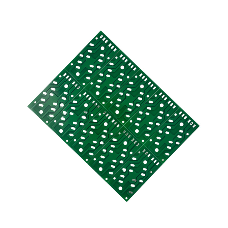
The realm of electronics manufacturing is built upon foundational components, and among the most fundamental of these is the single-sided printed circuit board (PCB). As the name implies, a single-sided PCB features a conductive copper layer on only one side of the substrate material. The other side is typically used for mounting components. This simple yet elegant design has been the cornerstone of the electronics industry for decades, enabling the mass production of reliable and cost-effective electronic devices. The manufacturing process involves laminating a thin layer of copper onto a non-conductive substrate, such as FR-4, CEM-1, or FR-1, followed by etching away unwanted copper to leave behind the desired circuit pattern. Holes are drilled for through-hole components, and a solder mask is applied to protect the copper traces, with a silkscreen layer added for component labels and identifiers. This straightforward process translates into significant advantages, particularly for high-volume, cost-sensitive applications where circuit complexity is low to moderate. For manufacturers specializing in these boards, the ability to deliver quickly and at scale is paramount. For instance, a company like Anhui Hongxin Electronic Technology Co., Ltd., with its extensive 20,000 square meter facility in the China PCB Industrial Park, exemplifies this capability. Their professional engineering team, leveraging over 15 years of experience, can streamline the production of single-sided boards, offering rapid prototyping and bulk order delivery within a remarkably short timeframe, ensuring that simple designs move from concept to market with incredible efficiency.
Five Key Long-Tail Keywords for Single-Sided PCB Enthusiasts
Navigating the world of PCB design and procurement requires an understanding of specific terminology. Focusing on precise, long-tail keywords can connect engineers, hobbyists, and procurement specialists with the exact information and services they need. These keywords often represent specific niches with dedicated traffic but lower competition, making them invaluable for targeted research. The following five terms are crucial for anyone working with or learning about single-layer circuit technology:
- single sided pcb design rules for beginners
- advantages and disadvantages of single layer pcb
- how to solder components on a single sided pcb
- single sided vs double sided pcb cost comparison
- where to manufacture prototype single sided pcb boards
Each of these phrases addresses a distinct stage in the lifecycle of a single-sided PCB, from initial design and evaluation to assembly, cost analysis, and finally, fabrication. In the following sections, we will delve deeply into each of these topics, providing comprehensive insights and practical guidance. The integration of these keywords into the discussion will provide a natural and informative flow, connecting specific user queries with detailed expert explanations. This approach is particularly beneficial when considering manufacturing partners, as companies that understand these nuanced topics, like Anhui Hongxin Electronic Technology Co., Ltd., are better positioned to offer not just fabrication, but valuable support throughout the entire process, from validating design rules to delivering finished prototypes and bulk orders.
Mastering Single-Sided PCB Design: Rules and Guidelines
Creating a functional and manufacturable single-sided PCB begins with a solid grasp of design principles. Adhering to single sided pcb design rules for beginners is not just a recommendation; it is a critical step to avoid costly manufacturing errors and ensure the reliability of the final product. The primary constraint of a single-layer board is the limitation of routing all electrical connections on one plane without the luxury of jumping to another layer with vias. This necessitates strategic planning of component placement and trace routing from the very beginning of the schematic capture and layout process.
Core Design Principles and Layout Strategies
The cornerstone of single-sided design is component placement. Designers must arrange components in a logical flow that minimizes trace crossover. This often involves grouping related components together and orienting integrated circuits (ICs) and connectors to facilitate straightforward routing. It is advisable to place all components on the top side (non-copper side) of the board, with their leads passing through drilled holes to be soldered onto the copper traces on the bottom side. When routing traces, one must always be mindful of clearance and creepage distances to prevent short circuits, especially in humid environments. Trace width is another vital parameter; it must be calculated based on the current carrying capacity to prevent overheating and trace failure. For standard signal traces, a width of 10-15 mils is common, but power and ground traces should be significantly wider, often 30-50 mils or more, depending on the current load.
Common Pitfalls and How to Avoid Them
Beginners often encounter several predictable challenges. One major issue is the unavoidable trace crossover, which cannot be solved with a via as on a double-sided board. The standard solution is to use a "jumper wire," a discrete wire soldered between two points on the board to bridge traces that cannot intersect on the copper layer. While effective, excessive use of jumpers can undermine the cost and assembly-time advantages of single-sided boards. Another frequent mistake is ignoring the manufacturer's Design for Manufacturability (DFM) guidelines. These guidelines specify minimum trace widths, spacing, hole sizes, and board edge clearances that the fabrication equipment can reliably produce. Submitting a design that violates these rules will lead to delays and additional engineering queries. Partnering with a manufacturer that provides clear DFM feedback is essential. A manufacturer with a strong engineering team, such as Anhui Hongxin Electronic Technology Co., Ltd., can offer invaluable pre-production consultations to review designs against their process capabilities, ensuring that a beginner's design is optimized for a smooth and successful fabrication run, whether it's a 24-hour prototype or a large-volume order.
Evaluating the Pros and Cons of Single-Layer PCBs
Choosing the right type of PCB for a project involves a careful trade-off analysis. A thorough understanding of the advantages and disadvantages of single layer pcb technology is crucial for making an informed decision that balances performance, complexity, and budget. This evaluation forms the basis for selecting the most appropriate platform for an electronic device, influencing everything from per-unit cost to repairability.
In-Depth Look at the Advantages
The benefits of single-sided PCBs are compelling, especially for a vast array of consumer and industrial applications. The most significant advantage is cost. The manufacturing process is simpler, requiring fewer materials (only one copper layer) and less complex processing steps like plating through-holes. This results in a lower cost per unit, which is magnified in high-volume production runs. The simplicity also translates to faster manufacturing lead times. Furthermore, the design and prototyping process is generally quicker and more straightforward, as the routing challenges are confined to one layer. This makes them an excellent choice for educational purposes and for hobbyists learning PCB design. From a reliability standpoint, having only one layer of traces can mean fewer potential points of failure, such as faulty vias or layer-to-layer delamination. They are also typically easier to repair and troubleshoot, as all connections are visible on one side of the board.
A Candid Assessment of the Limitations
However, the simplicity of single-sided boards comes with inherent limitations. The primary disadvantage is low circuit density. With all interconnections confined to a single plane, designing complex circuits becomes extremely challenging, if not impossible, due to the high likelihood of trace crossings. This restricts their use to relatively simple circuits with low component counts. The need for jumper wires to solve routing issues can increase assembly time and potentially reduce mechanical robustness. Additionally, the single-sided nature can lead to less optimal grounding and signal integrity in circuits sensitive to noise, as it is harder to implement a continuous ground plane. For high-frequency or high-speed digital applications, the lack of controlled impedance routing and shielding options makes single-sided boards unsuitable.
Comparative Analysis: Single-Sided vs. Multi-Layer PCBs
The following table summarizes the key differences to clarify the decision-making context. It's important to note that the choice is not about which is universally better, but which is more appropriate for a specific application's requirements and constraints.
| Feature | Single-Sided PCB | Double-Sided / Multi-Layer PCB |
|---|---|---|
| Circuit Complexity | Low to Moderate. Suitable for simple analog/digital circuits. | High. Can accommodate complex, high-density designs with microprocessors and BGAs. |
| Cost | Very Low per unit, especially in volume. Minimal material and process cost. | Higher. Cost increases with number of layers due to added materials and processing steps like lamination and via plating. |
| Design Flexibility | Low. Routing confined to one layer; jumpers often required. | Very High. Multiple layers allow for sophisticated routing, ground planes, and signal shielding. |
| Size & Density | Larger board area often required for a given circuit. | Can achieve a much smaller footprint for the same functionality. |
| Manufacturing Lead Time | Typically shorter due to simpler process. | Longer, especially as layer count increases. |
| Typical Applications | Calculators, power supplies, LED lighting, radio receivers, simple control boards. | Smartphones, computers, networking equipment, advanced automotive electronics. |
For projects where cost and simplicity are the driving factors, the single-sided PCB remains an unbeatable solution. Manufacturers that support a wide range of materials, from standard FR-1 to more specialized substrates, can tailor the board to specific environmental or electrical needs, further extending the applicability of this classic technology.
Practical Guide to Assembling Single-Sided Circuit Boards
Once a single-sided PCB is fabricated, the next critical phase is populating it with components. Knowing how to solder components on a single sided pcb is a fundamental skill for engineers, technicians, and makers. The process, while conceptually straightforward, requires attention to detail to create strong, reliable electrical and mechanical joints. The defining characteristic of assembly on a single-sided board is that all soldering is performed on the opposite side of the board from where the components are placed.
Step-by-Step Soldering Process and Techniques
The assembly process typically follows a logical sequence to ensure efficiency and prevent damage. It begins with inserting the smallest and lowest-profile components first, such as resistors, diodes, and jumper wires. The board is then flipped over to solder the protruding leads on the copper side. For through-hole components, the preferred method is hand soldering with a temperature-controlled iron or using wave soldering in a production environment. A good solder joint appears shiny, smooth, and concave, forming a "fillet" that covers the pad and flows onto the lead. It is crucial to use the appropriate solder alloy and flux. Lead-free solders require higher temperatures but are common in commercial products. After soldering, the excess lead length is trimmed flush with the solder joint to prevent shorts. For any surface-mount devices (SMDs) used on a single-sided board—which is less common but possible—reflow soldering or careful hand soldering with a fine tip is necessary. Throughout the process, electrostatic discharge (ESD) precautions should be taken when handling sensitive components like CMOS ICs.
Tools, Safety, and Inspection Best Practices
Having the right tools is half the battle. Essential equipment includes a good-quality soldering station with adjustable temperature, a variety of tip sizes, brass wool or a damp sponge for tip cleaning, fine-gauge solder (0.6mm-1.0mm diameter), flux, soldering aids (tweezers, clamps), and a well-lit, ventilated workspace. Safety cannot be overstated; proper ventilation or a fume extractor is mandatory to avoid inhaling solder fumes. After assembly, a rigorous inspection is required. This involves both visual inspection under magnification to check for common defects and electrical testing. Common defects to look for include:
- Cold solder joints: Dull, grainy, and lumpy appearance caused by insufficient heat or movement during cooling.
- Solder bridges: Accidental connections of solder between two adjacent traces or pads, causing a short circuit.
- Insufficient solder: The joint does not fully cover the pad, leading to a weak connection.
- Lifted pads: The copper pad detaches from the substrate due to excessive heat or mechanical stress during soldering or desoldering.
Functional testing with a multimeter (for continuity and shorts) and eventually powering the board with a current-limited supply is the final verification step. A manufacturer that provides high-quality boards with consistent solder mask application and accurate drill alignment, as ensured by certifications like ISO9001 and IATF16949 held by Anhui Hongxin Electronic Technology Co., Ltd., significantly simplifies the assembly process by reducing defects related to fabrication.
Cost Analysis: Single-Sided Versus Double-Sided PCB
Financial considerations are often the deciding factor in PCB selection. Conducting a single sided vs double sided pcb cost comparison reveals a multi-faceted picture where the base manufacturing cost is just one part of the equation. The total cost of ownership encompasses design effort, prototyping, assembly, testing, and potential redesigns. A clear breakdown helps in making a budget-conscious yet technically sound choice.
Breaking Down the Manufacturing Cost Drivers
The cost advantage of single-sided PCBs stems from a less resource-intensive production pipeline. The material cost is lower, as only one copper-clad laminate sheet is used. The processing steps are fewer: there is no need for plating through-holes (PTH) to connect two sides, no alignment for dual-side exposure, and generally simpler drilling and routing. This efficiency allows manufacturers to offer very competitive pricing, particularly for standard materials like FR-1, CEM-1, or FR-4. For bulk orders, this per-unit cost difference becomes substantial. In contrast, double-sided boards require a more complex process. After drilling, the holes must be metallized (plated) to establish electrical connectivity between the top and bottom layers. This involves multiple chemical baths and precise process control. The etching and registration for two layers also add complexity and potential yield loss. Consequently, the base price for a double-sided board of the same size and quantity is invariably higher.
Total Project Cost Considerations
However, viewing cost solely through the lens of the bare board price can be misleading. One must consider the total project cost. A single-sided board might be cheaper to fabricate, but if its design requires numerous jumper wires, the added component cost and increased manual assembly time can erode those savings. Furthermore, if the circuit complexity forces the use of a significantly larger single-sided board compared to a compact double-sided version, the cost of the larger substrate and the potential impact on product enclosure size must be factored in. For prototypes, the speed of iteration is also a cost factor. A single-sided design that is quick to layout and fabricate allows for faster design verification cycles. Manufacturers that offer rapid prototyping services, such as 24-hour delivery for double-sided prototypes mentioned by some, provide flexibility, but for true single-sided needs, the turnaround is often even quicker. The key is to engage with a manufacturer capable of producing both types. This allows for an unbiased consultation where a provider like Anhui Hongxin Electronic Technology Co., Ltd. can analyze your schematic and recommend the most cost-effective solution—whether it's a simple single-sided board delivered in 6-7 days for bulk orders or a more complex multilayer alternative—based on their expertise in fabricating everything from 1 to 32 layers.
Transforming a digital PCB layout into a physical board is a pivotal moment. For engineers and developers, knowing where to manufacture prototype single sided pcb boards involves evaluating a manufacturer's capabilities, quality, speed, and support beyond just the price quote. The prototype phase is where design flaws are caught and corrected, making the choice of fabrication partner critically important.
Essential Criteria for Selecting a Prototype Manufacturer
Several key factors should guide the selection process. First and foremost is manufacturing capability and quality assurance. Does the manufacturer have experience with the specific base material you require (e.g., standard FR-4, high-Tg, halogen-free, or metal-based)? Do they hold relevant international certifications like ISO9001, ISO14001, and UL, which provide independent verification of their quality and environmental management systems? Second, evaluate their technical support and communication. A manufacturer with a strong engineering team, such as the over 7 professional engineers with 15+ years of experience at Anhui Hongxin Electronic Technology Co., Ltd., can provide proactive DFM checks and offer solutions to potential design issues before production begins, saving time and cost. Third, consider their speed and flexibility. Prototyping is an iterative process, so fast turnaround times are invaluable. Look for clear timelines for different service tiers. The ability to handle both small-batch prototypes and seamlessly scale to volume production is a significant advantage, as it avoids the need to requalify a new supplier later.
The Prototype Journey: From Gerber Files to Finished Boards
The process typically begins with the submission of design files (usually Gerber and drill files) along with specifications for material, thickness, copper weight, solder mask color, and surface finish (like HASL, ENIG, or immersion tin). A reputable manufacturer will promptly provide a detailed quote and a manufacturability review. Once approved, fabrication commences. For a single-sided prototype, the steps include material cutting, drilling, copper patterning (through print and etch), solder mask application, silkscreen printing, surface finishing, and electrical testing. A trustworthy manufacturer will keep you informed throughout this process. Upon completion, the boards are shipped. It is prudent to order a few extra prototypes to account for assembly errors during testing. The final step is to thoroughly test the prototype under real-world conditions to validate the design. Choosing a manufacturer with a comprehensive portfolio, from simple single-sided to advanced HDI and rigid-flex boards, indicates a broad expertise that can be leveraged for advice and future projects, ensuring a reliable partnership as your product evolves from a simple prototype to a high-volume commercial device destined for global markets.


 LET'S CREATE THE FUTURE TOGETHER

Contact Us Anytime
Copyright © Anhui Hongxin Electronic Technology Co., Ltd. All Rights
Reserved.
privacy
Wholesale Printed Circuit Board Suppliers, Manufacturers
![]()
