


 English
 Español
 Français

AI Computing Boom Pushes High-Layer & High-Speed PCB Demand to New Heights in 2026
The global printed circuit board (PCB) industry is entering one of its strongest structural upcycles in decades, driven overwhelmingly by the buildout of generative AI data centers. According to market analyst Prismark, worldwide PCB production value is projected to exceed $102 billion in 2026, with AI server and high-speed networking boards identified as the fastest-growing segment — outpacing consumer electronics, automotive, and industrial segments.
The demand step-change comes directly from the architecture of AI compute. Unlike conventional enterprise servers, which typically use 8–12 layer motherboards, a single high-end AI server can carry 30 to 50 layers, and flagship accelerator boards and switch backplanes may reach 70–100 layers. A single AI server also consumes roughly 8 to 10 times the PCB value of a standard server, because the board must simultaneously support massive parallel data channels, high-power delivery, and dense connector arrays.
These boards place stringent demands on both materials and fabrication. Signal speeds now run at 112 Gbps per channel and are heading toward 224 Gbps, which forces designers to move from traditional FR-4 to ultra-low-loss dielectric materials such as Megtron 6/7, Tachyon 100G, or equivalent low-Df, low-Dk laminates. Tight impedance control, controlled dielectric thickness, smooth very-low-profile copper foil, and precise transmission-line modeling are no longer optional — they are baseline requirements for signal integrity at high frequency.
Fabricating such boards introduces new process constraints. As layer counts climb, layer-to-layer registration accuracy, lamination alignment, and via-stub management (including precision back-drilling) become critical. Designers are increasingly combining high-layer construction with HDI fine-line structures and via-in-pad technology to route dense high-speed signals without an uncontrolled escalation in layer count. Thermal management is equally demanding: high-power GPUs and HBM memory packages require robust copper weights and dense thermal via arrays to dissipate heat reliably.
Capacity is now the bottleneck. Leading PCB manufacturers are rushing to expand high-layer and high-speed production lines, but qualified equipment, low-loss material supply, and experienced process engineers cannot be added overnight. As a result, lead times for premium high-speed PCBs have stretched to several months, and order backlogs are now carried into 2027. Standard and mid-complexity FR-4 boards, by contrast, remain comparatively available.
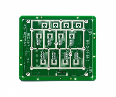
For procurement teams and hardware design managers, this environment rewards early planning. Starting DFM (Design for Manufacturability) reviews early in the design cycle, locking in material choices, and engaging the PCB supplier before tape-out can prevent costly redesigns and long delays. Buyers who treat PCB as a long-lead, strategic component — rather than a commodity purchased at the last minute — are better positioned to secure capacity and protect product launch schedules.
The AI-driven PCB boom is expected to persist through the decade, as data center operators continue to scale GPU clusters and as AI workloads expand from training toward inference, edge computing, and industrial AI. For PCB manufacturers with high-layer, high-speed, and HDI capabilities, this represents a multi-year growth runway; for buyers, it underscores the lasting value of a qualified, technically capable supply partner.

 LET'S CREATE THE FUTURE TOGETHER

Contact Us Anytime
Copyright © Anhui Hongxin Electronic Technology Co., Ltd. All Rights
Reserved.
privacy
Wholesale Printed Circuit Board Suppliers, Manufacturers

