


 English
  Español
  Français
Multilayer PCB Manufacturing, Stackup Design & Cost Guide
Content
What Is a Multilayer PCB?
A multilayer PCB is a printed circuit board built from three or more conductive copper layers separated by insulating dielectric material and pressed together into a single rigid structure. Anywhere a design needs more routing density, better signal integrity, or controlled impedance than a single- or double-sided board can deliver, a multilayer PCB is the standard answer — from smartphone motherboards to server backplanes to automotive radar modules.
The core advantage over a two-layer board isn't just extra routing space. Internal layers can be dedicated entirely to power and ground planes, which shortens return paths, reduces electromagnetic interference, and stabilizes voltage delivery to high-speed components — none of which is achievable on a board with only top and bottom copper.
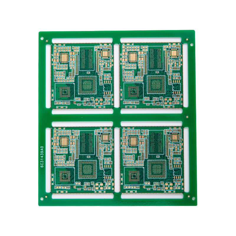
Multilayer PCB Manufacturing and Fabrication Process
Building a multilayer board is fundamentally a sequence of building, bonding, and drilling through individual copper-clad layers until they become one solid structure. The core steps are consistent across 4-layer, 6-layer, and higher-count boards, though the number of lamination cycles and drilling passes scales with layer count.
- Inner layer imaging and etching: Each internal copper layer starts as a copper-clad laminate core. A photoresist is applied, exposed with the circuit pattern, developed, and the exposed copper is etched away, leaving the internal trace and plane pattern.
- Automated optical inspection (AOI): Every inner layer is scanned against the design file before lamination, since a defect trapped inside the stack after pressing can't be repaired.
- Layer alignment and lamination: Inner layers, prepreg (uncured, resin-impregnated fiberglass sheets), and outer copper foil are stacked in the designed sequence, pinned for registration, then pressed under heat and pressure. The prepreg melts and cures, permanently bonding the stack into a single rigid panel.
- Drilling: Mechanical or laser drilling creates the through-holes and vias that will electrically connect different layers. Laser drilling is used for the very small microvias common in high-density designs, while mechanical drilling handles standard through-holes.
- Through-hole plating (PTH): Drilled holes are chemically cleaned and then electroplated with copper, creating a conductive barrel that links traces on different layers together.
- Outer layer imaging and etching: The outer copper layers go through the same photoresist, expose, develop, and etch cycle as the inner layers, defining the final surface circuit pattern.
- Solder mask and silkscreen: A solder mask is applied to protect copper from oxidation and prevent solder bridging, followed by silkscreen printing for component labels and reference designators.
- Surface finish: A finish such as HASL, ENIG, or OSP is applied to exposed copper pads to protect them until assembly and to provide a solderable surface.
- Electrical testing and final inspection: Flying probe or bed-of-nails testing verifies every net against the design netlist, followed by a dimensional and visual final inspection before the board ships.
For boards with more than roughly 8 layers, this process often repeats in stages — an initial lamination of a sub-stack, followed by additional drilling and lamination cycles to build up the full layer count, which is what separates standard multilayer fabrication from the sequential build-up processes used in HDI boards.
Multilayer PCB Stackup and Layer Design
A PCB stackup is the specific arrangement and sequence of copper layers, dielectric thickness, and prepreg used to build the board, and it directly determines the board's electrical performance, manufacturability, and cost. Getting the stackup right is arguably more consequential to a design's success than the schematic itself, because a poorly planned stackup can introduce signal integrity problems that no amount of routing skill can fully correct afterward.
A few principles guide most stackup decisions:
- Keep signal layers adjacent to a reference plane. Every signal layer should sit next to an unbroken ground or power plane to give high-speed signals a continuous, low-inductance return path.
- Maintain symmetry. A stackup that isn't mirrored top-to-bottom in copper weight and dielectric thickness tends to warp during lamination as the two halves cure and cool at different rates.
- Pair power and ground planes closely. Placing power and ground planes on adjacent layers with a thin dielectric between them creates useful interplane capacitance that helps filter high-frequency noise.
- Control impedance deliberately. Trace width, copper thickness, and dielectric height between a trace and its reference plane must be calculated together to hit a target impedance (commonly 50Ω single-ended or 90/100Ω differential), not adjusted after the fact.
4-Layer vs. 6-Layer PCB Manufacturing
A 4-layer PCB is the most common entry point into multilayer manufacturing and typically follows a signal-ground-power-signal stackup, giving two dedicated reference planes while keeping cost close to a well-built double-sided board. It's the standard choice for moderately dense designs that need better EMI control and impedance consistency than two layers can offer, without the added lamination cycles of higher layer counts.
A 6-layer PCB adds a second signal layer pair or an additional plane, commonly arranged as signal-ground-signal-signal-power-signal or a variant with two ground planes, which gives designers more routing layers while keeping every signal layer adjacent to a return path. Six-layer boards are the typical jump point for designs with higher pin-count BGAs, multiple high-speed interfaces, or enough routing congestion that a 4-layer board would force too many trace-width compromises.
| Factor | 4-Layer PCB | 6-Layer PCB |
|---|---|---|
| Typical stackup | Signal / Ground / Power / Signal | Signal / Ground / Signal / Signal / Power / Signal |
| Routing density | Moderate | High |
| Lamination cycles | 1 | 1–2 |
| Typical use case | General embedded systems, consumer electronics | Higher-density boards, multiple high-speed interfaces |
High-Density Multilayer PCBs
High-density multilayer PCBs, often built using HDI (high-density interconnect) techniques, push far beyond standard multilayer construction to fit more connections into less board area. Instead of drilling through-holes that span the entire board thickness, HDI boards use laser-drilled microvias — typically under 150 microns in diameter — that connect only adjacent layers, along with finer trace and space geometries down to 3 mil or less.
These boards are built up in sequential lamination stages rather than a single press cycle, which is what allows microvias to be stacked or staggered between layer pairs. The result is a board that can route fine-pitch BGA packages with 0.4mm or 0.3mm ball pitch, which standard through-hole vias are physically too large to escape from without consuming excessive board space.
Multilayer PCB Applications
Multilayer PCBs show up wherever a design needs more than basic routing — the layer count and stackup complexity generally scale with how demanding the electrical and space requirements are.
- Consumer electronics: Smartphones, tablets, and wearables rely on high layer counts and HDI construction to pack dense circuitry into extremely limited board area.
- Telecommunications and networking: Routers, switches, and 5G infrastructure equipment use multilayer boards with controlled impedance to support high-speed serial links and dense connector routing.
- Automotive electronics: ADAS modules, infotainment systems, and engine control units use multilayer PCBs rated for vibration and thermal cycling well beyond typical consumer specs.
- Medical devices: Diagnostic and monitoring equipment depend on multilayer boards for signal integrity in low-noise analog front ends alongside digital processing.
- Aerospace and defense: High-reliability multilayer boards, often with 10+ layers, support radar, avionics, and communication systems that must perform in extreme environmental conditions.
- Industrial control systems: PLCs, motor drives, and power conversion equipment use multilayer boards to isolate noisy power sections from sensitive control circuitry.
What Drives Multilayer PCB Cost
Multilayer PCB cost is driven by a combination of layer count, material selection, and manufacturing complexity, and understanding which factors move the needle most helps in making cost-effective design decisions early rather than after layout is finished.
- Layer count: Cost doesn't scale perfectly linearly, but each additional layer pair adds material, an additional imaging and etching cycle, and additional lamination and drilling steps, so jumping from 4 to 8 layers roughly doubles material and process cost rather than simply adding a fixed increment.
- Base material: Standard FR-4 is the cost baseline; high-frequency laminates (such as PTFE-based materials for RF applications) or high-Tg materials for thermally demanding boards carry a significant material premium.
- Hole complexity: Microvias, blind and buried vias, and very small aspect-ratio through-holes require laser drilling and additional plating steps that cost more than standard mechanical through-hole drilling.
- Trace and space tolerance: Pushing below roughly 4 mil trace/space requires tighter process control and lower manufacturing yield, which raises unit cost, particularly at low production volumes.
- Surface finish: ENIG and other gold-based finishes cost more than HASL or OSP but are often necessary for fine-pitch components or long shelf life before assembly.
- Order volume and lead time: Prototype and low-volume runs carry a higher per-board cost due to setup and tooling amortization, while expedited turnaround times add a further premium on top of standard pricing.
Recommended Products

 LET'S CREATE THE FUTURE TOGETHER

Contact Us Anytime
Copyright © Anhui Hongxin Electronic Technology Co., Ltd. All Rights
Reserved.
privacy
Wholesale Printed Circuit Board Suppliers, Manufacturers

