

 English
  Español
  Français
Comprehensive Guide to Double-sided PCB: Design, Manufacturing, and Troubleshooting
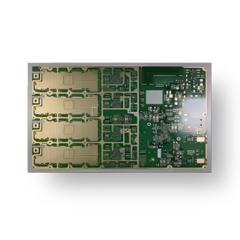
In modern electronic products, printed circuit boards (PCBs) play a crucial role, and Double-sided PCB is one of the most common high-density PCB types. Compared to single-sided PCBs, double-sided PCBs can accommodate more circuits in the same area and offer greater design flexibility. This makes them widely used in communication devices, industrial control boards, automotive electronics, and various consumer electronics.
This article will provide a comprehensive guide on the design, manufacturing, soldering, and troubleshooting methods of Double-sided PCB, helping engineers and DIY enthusiasts systematically master double-sided PCB technology.
Content
Section 1: Basics of Double-sided PCB
Structure and Features of Double-sided PCB
Double-sided PCB refers to a PCB with circuits laid out on both sides of the board. Typically, a double-sided PCB consists of several key layers:
- Substrate Layer: Usually made of FR-4 fiberglass epoxy resin, providing mechanical support and insulation.
- Copper Layer: Copper foil is applied on both sides of the board for electrical connections.
- Solder Mask: Protects copper traces from oxidation and prevents solder bridges.
- Silkscreen: Labels component positions, part numbers, and other markings.
The main features of double-sided PCBs include higher circuit density, improved electrical performance, and flexible design that allows key components to be placed on different layers, saving space.
Difference Between Single-sided and Double-sided PCB
| Feature | Single-sided PCB | Double-sided PCB |
| Number of Layers | One | Two |
| Component Layout | Limited | Flexible |
| Cost | Lower | Higher (more complex manufacturing) |
| Applications | Simple electronic products | High-density electronic products |
Compared to single-sided PCBs, double-sided PCBs have obvious advantages in high-density designs but also introduce more challenges in manufacturing and soldering. Therefore, mastering double-sided PCB soldering techniques and circuit design principles is essential for engineers.
Applications of Double-sided PCB in Electronic Products
Double-sided PCBs are widely used in electronic products that require high reliability and complex functionality. Typical applications include communication devices such as routers and base station modules, industrial control boards such as PLC controllers and motor drivers, automotive electronics like instrument panels and sensor modules, and consumer electronics such as smartwatches and portable audio devices.
Clearly, the design of a Double-sided PCB affects not only circuit performance but also the maintainability and lifespan of the product.
Section 2: Design Considerations for Double-sided PCB
Key Points in Double-sided Circuit Design
When designing circuits for double-sided PCBs, several critical factors must be considered. Via design is particularly important for connecting circuits on both sides of the board. The diameter of the via should match the current requirements to prevent overheating. Additionally, signal layers should be carefully arranged to ensure proper electrical performance, and power and ground planes should be continuous to minimize noise.
Component Layout and Routing Techniques
In double-sided PCB design, proper component placement and routing order are crucial. Components with similar functions should be placed close together to shorten critical paths, and high-frequency components should be separated to avoid interference. Signal traces should follow the shortest path possible, avoid sharp 90-degree turns, and maintain consistent impedance to reduce reflection and crosstalk.
Signal Integrity and Electromagnetic Compatibility
Double-sided PCBs are prone to signal integrity and electromagnetic compatibility issues in high-speed designs. Reflections, crosstalk, and impedance mismatches can occur. To mitigate these problems, designers use controlled trace widths, maintain trace length symmetry, and ensure proper grounding. Ground planes and filtering capacitors also help reduce electromagnetic interference (EMI).
Section 3: Manufacturing Process of Double-sided PCB
Overview of PCB Manufacturing Process
The manufacturing process of a double-sided PCB is more complex than that of a single-sided board. It includes design transfer using Gerber files, circuit pattern printing with photolithography, drilling and plating through-holes to connect layers, etching to remove excess copper, solder mask application, silkscreen printing, and final testing for electrical continuity and visual inspection.
Materials and Substrate Selection
Common materials for double-sided PCBs include FR-4 for general-purpose applications, CEM-1/CEM-3 for cost-effective solutions, and high-frequency materials like PTFE for high-speed circuits. Material selection should consider operating temperature, electrical performance, and compatibility with manufacturing processes.
Drilling, Copper Plating, and Surface Finishing
Precision drilling creates holes for vias and components, followed by copper plating to establish electrical connections between layers. Surface finishes like HASL, immersion gold, or OSP protect copper pads and improve solderability. Proper process control is essential to ensure the reliability and longevity of a Double-sided PCB.
Common Manufacturing Issues
Manufacturing defects can include short circuits due to insufficient solder mask, open circuits from incomplete plating, warping from uneven lamination, and through-hole connectivity issues. Strict process control, careful inspection, and quality testing are critical to prevent these issues and ensure high yield rates.
Section 4: Soldering and Assembly of Double-sided PCB
Soldering double-sided PCBs is more challenging than single-sided boards due to the placement of circuits on both sides. High-density layouts, multiple vias, and a combination of surface-mount and through-hole components increase the complexity. The key principle in soldering is to ensure reliable connections without short circuits while avoiding thermal or mechanical damage to the board.
During manual soldering, one side of the PCB is soldered first, securing critical components before flipping the board for the other side. In mass production, reflow soldering is preferred for surface-mount devices, and wave soldering is used for through-hole components. Temperature control is crucial to prevent board warping or solder joint defects. Component placement order is also important; heat-sensitive components are soldered first, and larger components last. Using flux improves wetting and joint strength, while visual and X-ray inspections help detect hidden soldering defects.
Section 5: Troubleshooting Double-sided PCB
Even with careful design and manufacturing, double-sided PCBs may experience various electrical issues, including open circuits, short circuits, signal attenuation, power noise, or localized overheating. Effective troubleshooting requires a comprehensive understanding of the board’s functional sections, such as power, signal processing, and interface areas.
Typical methods include measuring resistance, voltage, and continuity with a multimeter, observing signals with an oscilloscope, and using infrared thermal imaging to detect hot spots. Problems often arise in vias or through-hole connections, which can cause intermittent failures or non-functional circuits. High-frequency designs may also face signal interference or crosstalk. Environmental factors such as temperature changes or mechanical stress can create micro-cracks, leading to intermittent faults. Standard troubleshooting procedures involve visual inspection, electrical testing, targeted rework or soldering, and component replacement when necessary.
Case Study
Consider a communication module with a double-sided PCB: high-frequency circuits were placed on the top layer, power and ground planes on the bottom, connected via multiple through-holes. During testing, intermittent signal failures occurred in the high-frequency section. Upon microscopic inspection, some vias were found with uneven copper plating, causing poor connections. After re-plating and re-soldering the affected vias, the module functioned correctly. This example illustrates that while double-sided PCB design allows high-density layouts, it also increases manufacturing and troubleshooting complexity.
Conclusion
Through a comprehensive analysis of Double-sided PCB, it is clear that double-sided PCBs play a central role in electronic products and require advanced technical skills. From structural understanding to design principles, manufacturing processes, soldering techniques, and troubleshooting methods, every aspect of a double-sided PCB requires meticulous attention.
Mastering design and soldering techniques allows for high-density layouts and improved product performance, while systematic troubleshooting ensures reliability and stability. As electronic products continue to demand higher performance and integration, the importance of double-sided PCB technology will continue to grow. Engineers, hobbyists, and product designers who fully understand Double-sided PCB technology will gain a significant advantage in creating high-quality, reliable electronic products.
Recommended Products


 LET'S CREATE THE FUTURE TOGETHER

Contact Us Anytime
Copyright © Anhui Hongxin Electronic Technology Co., Ltd. All Rights
Reserved.
privacy
Wholesale Printed Circuit Board Suppliers, Manufacturers
![]()
