

 English
  Español
  Français
How Does a Double Sided PCB Differ from a Single Sided PCB?
Content
The Foundational Divide in Circuit Board Design
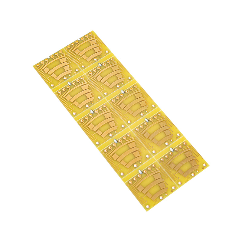
The world of electronics is built upon a simple yet critical foundation: the Printed Circuit Board (PCB). At the most fundamental level, the choice between single-sided and double-sided PCBs shapes the functionality, complexity, and cost of virtually every electronic device. A single-sided PCB has conductive copper traces on only one side of the insulating substrate, while a double-sided PCB, as the name implies, features conductive layers on both sides of the board. This seemingly simple difference creates a profound divergence in design possibilities, manufacturing processes, and application suitability. Understanding this core distinction is essential for anyone involved in electronics, from hobbyists to professional designers, as it directly impacts the feasibility and performance of a project. The evolution from single to double-sided boards marked a significant leap in electronics, enabling more compact and powerful devices by effectively doubling the available routing area without increasing the board's physical footprint. This article will delve deep into the technical, practical, and economic contrasts between these two board types, providing a comprehensive guide to inform your design choices.
Core Structural and Manufacturing Differences
The primary distinction between these PCBs lies in their physical architecture, which dictates entirely different manufacturing workflows and design constraints.
Layer Composition and Base Materials
A single-sided PCB consists of a single layer of conductive copper foil laminated onto one side of a non-conductive substrate, typically FR-4 fiberglass. The other side is bare substrate, often used for component placement. In contrast, a double-sided PCB has copper foil laminated onto both sides of the substrate. This fundamental difference in layer count is the origin of all other variations. Both types may use similar base materials—FR-4 being the most common for its excellent mechanical strength and electrical insulation properties—but the double-sided board requires a more sophisticated bonding process to ensure the copper layers adhere reliably to both surfaces. The substrate must maintain dimensional stability and withstand the thermal stresses of having conductive pathways and components on both sides. Furthermore, the choice of substrate thickness can be more critical for double-sided boards, especially when considering impedance control or mechanical rigidity for larger boards with components on both sides.
The Crucial Role of Vias and Plated-Through Holes
This is arguably the most significant manufacturing and functional differentiator. In a single-sided PCB, all electrical connections are made on the one copper layer. Components are typically inserted through holes and soldered to pads on the same side, with no electrical connection needed to the other side of the board.
For a double-sided PCB to function, the circuits on the top and bottom layers must be interconnected. This is achieved through vias in double sided PCB fabrication. A via is a small hole drilled through the board and the substrate, which is then plated with a conductive material, usually copper, creating an electrical pathway between the two layers. The creation of these plated-through holes (PTH) is a complex, multi-step electrochemical process that defines double-sided PCB manufacturing:
- Drilling: Precise holes are drilled through the entire board stack at locations specified in the design files.
- Desmear and Etch-back: This chemical process cleans the hole walls of resin smear from drilling and micro-etches the exposed fiberglass to ensure optimal adhesion for the copper plating.
- Electroless Copper Deposition: A thin, catalytic layer of copper is chemically deposited onto the hole walls and the entire board surface, making it conductive for the subsequent electroplating step.
- Electroplate Copper: The board is immersed in an electrolyte solution, and through electrolysis, a thicker, more durable layer of copper is plated onto the hole walls and surface traces, solidifying the connection.
The existence of this PTH process makes double-sided board fabrication more expensive and time-consuming but unlocks a new dimension in routing density. Without reliable vias, a double-sided board would simply be two independent single-sided boards glued back-to-back, which is not functionally useful for complex circuits.
Design Complexity and Routing Capabilities
The available routing space directly dictates the complexity of the circuit that can be implemented. This is where the choice between single and double-sided becomes a critical design decision.
Trace Routing and Circuit Density
On a single-sided board, all traces must exist on one plane without crossing each other to create short circuits. This often necessitates creative and sometimes lengthy routing paths, using jumper wires to bypass intersecting traces, or significantly limiting the circuit's complexity. The design is essentially a two-dimensional puzzle with severe constraints.
Double-sided PCBs introduce a third dimension. A trace can start on the top layer, travel through a via, and continue its path on the bottom layer, allowing it to cross over another trace on the top layer without making contact. This capability dramatically increases routing freedom. Designers can use one layer primarily for horizontal traces and the other for vertical traces, or segregate analog and digital signals, power and ground planes, or input and output sections. This layered approach is the cornerstone of modern, dense circuit design. For instance, a common strategy is to use one copper layer as a dedicated ground plane, which improves signal integrity and reduces electromagnetic interference (EMI), a luxury rarely possible with single-sided layouts. The increased density directly supports more components and more sophisticated functionality in a smaller area, a key demand in today's miniaturized electronics.
Component Placement and Assembly
Component placement logic also diverges significantly. In traditional single-sided through-hole design, all components are placed on the non-copper side, with their leads bent and inserted through holes to be soldered onto the copper traces on the opposite side. This limits placement to one side of the board.
Double-sided PCBs enable double sided pcb assembly techniques for both through-hole and surface-mount devices (SMD). Components can be placed on both sides of the board.
- Through-Hole on Both Sides: While less common, it's possible to have through-hole components on both sides. This requires careful sequencing in the soldering process (often wave soldering for the primary side and selective or hand soldering for the secondary) to prevent components from falling off during assembly.
- Surface-Mount Technology (SMT) Dominance: The real advantage is with SMD components. Small, leadless components can be easily soldered onto pads on either side of the board using reflow soldering. This allows for a tremendous increase in component density. A designer can place large integrated circuits (ICs) and passive components on the top side, and smaller resistors, capacitors, and diodes on the bottom side, optimizing space usage. This is a critical technique for creating compact consumer electronics like smartphones and wearables. The assembly process for double-sided SMT boards involves applying solder paste, placing components, and then reflowing one side at a time, often starting with the side that has smaller or fewer components.
Electrical Performance and Reliability Considerations
The architectural differences extend beyond physical layout to influence how the board behaves electrically and how reliably it operates over time.
Signal Integrity and Noise
Single-sided boards are more susceptible to electromagnetic interference (EMI) and crosstalk. With all traces on one layer and typically no dedicated ground plane, noise from one trace can easily couple into adjacent traces. They also act more effectively as antennas, both emitting and receiving interference. Managing return paths for signals is challenging, which can lead to signal integrity issues, especially at higher frequencies or in circuits with sensitive analog components.
The double-sided board offers superior tools for managing electrical performance. The use of a solid ground plane on one layer (a common practice) provides several key benefits:
- Shielding: The ground plane acts as a shield between noisy and sensitive circuits on the opposite layer.
- Controlled Impedance: It creates a predictable return path for signals, which is essential for maintaining signal integrity in digital and high-frequency analog circuits.
- Reduced EMI: By providing a low-inductance path for high-frequency currents, it minimizes electromagnetic emissions.
- Improved Thermal Dissipation: The additional copper layer helps spread and dissipate heat from components.
However, these benefits are not automatic; they must be designed for. Poor via placement can create ground loops, and splitting planes incorrectly can worsen performance. Thus, while the potential for better electrical performance is high, it requires more expertise to realize.
Mechanical Robustness and Failure Points
A single-sided PCB is mechanically simpler. Its primary failure points are trace lifts (where a copper trace peels from the substrate) and broken solder joints. The lack of plated-through holes means there are no internal barrel cracks to worry about.
The double-sided PCB, while offering more redundancy in some areas (like dual-sided attachment for some components), introduces the via as a potential failure point. The copper plating inside the via barrel is relatively thin and can be susceptible to cracking due to thermal expansion stresses during soldering or in environments with large temperature swings. This is a key consideration for thermal management in double layer PCB design. Proper thermal relief patterns in pads connected to ground planes, adequate copper balancing to prevent warping, and appropriate via sizing are all critical to ensuring the long-term reliability of a double-sided board. Furthermore, the board must be designed to withstand the mechanical stress of having heavier components mounted on both sides, potentially requiring additional support or stiffer substrate material.
Cost Analysis and Application Suitability
The decision often boils down to a trade-off between performance, complexity, and cost. Understanding the total cost of ownership is crucial.
Direct Cost Comparison and Fabrication Lead Time
Below is a breakdown of the key cost and time drivers that differentiate the two board types.
| Cost/Time Factor | Single-Sided PCB | Double-Sided PCB |
|---|---|---|
| Base Material Cost | Lower (less copper, simpler laminate) | Higher (more copper, processing for two sides) |
| Manufacturing Process Steps | Simpler: patterning, etching, drilling, solder mask/silkscreen. Drilling is non-plated. | More complex: Requires all steps for single-sided plus plated through hole process steps: drilling, desmear, electrodes copper, electroplating. |
| Typical Fabrication Lead Time | Shorter (fewer process steps, higher industry capacity for basic boards) | Longer (more steps involved, especially plating) |
| Assembly Cost | Generally lower. Often only one side to populate, simpler soldering process. | Can be higher. Potential for two-sided assembly, requiring multiple soldering passes or more complex fixtures. |
| Design and Tooling Cost | Lower. Simpler design rules, less simulation needed. | Higher. Requires careful via placement, layer management, and potentially signal integrity analysis. |
While the per-unit cost of a double-sided board is higher, it can lead to overall system cost savings by enabling a smaller overall board size, reducing the product enclosure size, and improving yield by allowing a more logical and less congested layout that is easier to test and debug.
Ideal Applications for Each Type
The choice is application-driven. The question of when to use double sided vs single sided pcb is answered by the project's requirements.
Typical Single-Sided PCB Applications:
- Simple Educational Kits and Hobbyist Projects: Where cost is the primary constraint and complexity is low (e.g., basic LED circuits, simple timers).
- High-Volume, Low-Functionality Consumer Goods: Where every cent matters, such as in simple toys, basic power supplies, or calculator boards.
- Relays and Power Control Boards: Where components are large, traces are wide for high current, and circuit density is not an issue.
- Certain Automotive Modules: For non-critical, simple functions like basic lighting control.
Typical Double-Sided PCB Applications:
- Consumer Electronics: Almost universally used in devices like routers, set-top boxes, smart home devices, and audio equipment.
- Industrial Control Systems: Where reliability and moderate circuit density are required for motor drivers, sensor interfaces, and programmable logic controllers (PLCs).
- Telecommunications Modules: Requiring better signal integrity and grounding than single-sided boards can offer.
- Medical Devices (non-implantable): Where compact size and reliability are key, such as in patient monitors or diagnostic tools.
- Automotive Electronics (ECUs, Infotainment): For engine control units, dashboard clusters, and other systems requiring robust performance in harsh environments.
For more demanding applications, designers often evaluate advantages of double layer pcb for power electronics. In power circuits, the second layer can be used as a continuous, uninterrupted plane for power or ground. This drastically reduces trace inductance and resistance, allowing for higher current carrying capacity, better voltage regulation, and improved thermal performance by spreading heat across a large copper area. It also provides shielding for sensitive control circuitry on the opposite layer from noisy switching elements like MOSFETs and inductors.
Making the Informed Choice for Your Project
Selecting the appropriate PCB type is a foundational decision. Start by thoroughly defining your project requirements: circuit complexity (component count and interconnectivity), required physical size, electrical performance needs (signal speed, noise sensitivity, current levels), operating environment (thermal, mechanical stress), and of course, the target unit cost. For simple, cost-sensitive, or high-current/low-frequency projects, a single-sided PCB may be perfectly adequate and the most economical choice. However, if your design involves microcontrollers, digital logic, analog sensors, power regulation, or needs to fit into a small enclosure, the routing flexibility, noise immunity, and density advantages of a double-sided PCB will almost certainly be necessary. While it incurs a higher initial fabrication cost, it often prevents costly design compromises, reduces debugging time, and results in a more professional, reliable, and performant end product. The key is to match the board's capabilities to the circuit's demands without over-engineering or under-specifying.


 LET'S CREATE THE FUTURE TOGETHER

Contact Us Anytime
Copyright © Anhui Hongxin Electronic Technology Co., Ltd. All Rights
Reserved.
privacy
Wholesale Printed Circuit Board Suppliers, Manufacturers
![]()
