

 English
  Español
  Français
Single, Double & Multilayer PCB: Types and How to Choose
Single-sided PCBs are the right choice for simple, low-cost applications; double-sided PCBs suit moderate complexity with budget constraints; and multilayer PCBs are essential for high-density, high-speed, or noise-sensitive designs. These three PCB types represent a progression in manufacturing complexity, capability, and cost—each with a clearly defined set of applications where it delivers the best outcome. A single-sided board that costs $0.50 to produce is the correct engineering and commercial decision for a basic LED controller; that same board would be an impractical starting point for a 5G modem. Understanding the structural, electrical, and manufacturing differences between these three categories is the foundation for making sound PCB decisions from the earliest design stage.
Content
- 1 How PCB Layer Count Defines Capability
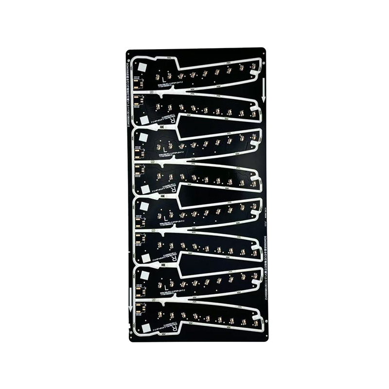
- 2 Single-Sided PCB: Structure, Strengths, and Ideal Applications
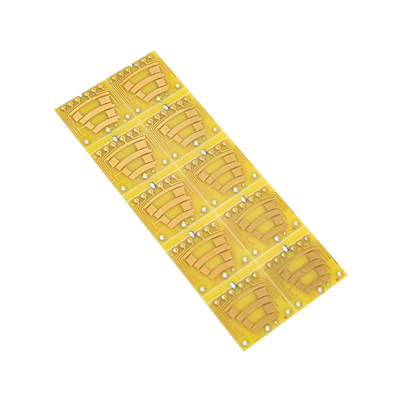
- 3 Double-Sided PCB: Increased Density and Broader Application Range
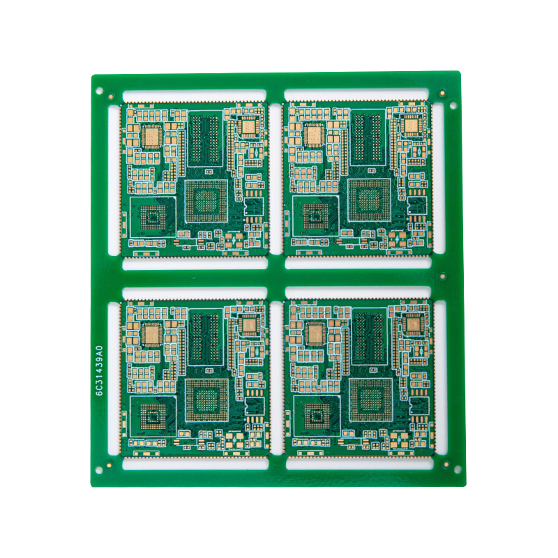
- 4 Multilayer PCB: High Density, High Performance, and Signal Integrity
- 5 Direct Comparison: Single-Sided vs Double-Sided vs Multilayer PCB
- 6 How to Choose the Right PCB Type for Your Design
- 7 PCB Design Rules and Minimum Feature Sizes by Board Type
How PCB Layer Count Defines Capability
A printed circuit board is a laminated structure of conductive copper layers separated by insulating substrate material—most commonly FR4 glass-epoxy laminate. The number of copper layers determines how many independent routing channels exist within the board, which in turn governs routing density, signal integrity, power distribution quality, and electromagnetic compatibility (EMC) performance.
The three fundamental layer configurations each represent a distinct engineering capability tier:
- Single-sided PCB (1 copper layer): All conductive traces are on one side of the substrate. Component mounting and trace routing occupy the same plane, limiting routing density to what can be achieved without crossovers.
- Double-sided PCB (2 copper layers): Copper traces exist on both faces of the substrate, connected through plated-through holes (PTH). Components can be mounted on one or both sides, roughly doubling routing capacity relative to single-sided boards.
- Multilayer PCB (4+ copper layers): Multiple copper layers are laminated into a single board structure with internal routing layers, dedicated power planes, and ground planes. Layer counts range from 4 to 50+ in advanced applications, with 4, 6, 8, and 10 layers being the most common commercial configurations.
The Role of Substrate Material
All three PCB types use the same base substrate options, though material selection becomes more critical as layer count increases. FR4 (glass-reinforced epoxy, Tg 130–170°C) is the standard for the majority of commercial and industrial applications. High-frequency designs above 1 GHz increasingly require low-loss laminates such as Rogers 4003C (dielectric constant εr = 3.55, loss tangent 0.0027) or Isola IS680 to maintain signal integrity across multiple layers—a consideration that does not arise in most single-sided applications.
Single-Sided PCB: Structure, Strengths, and Ideal Applications
A single-sided PCB has one layer of copper foil bonded to one face of the insulating substrate. Components are typically mounted on the copper side (for through-hole components, lead wires pass through the board and are soldered on the copper side) or on the bare substrate side with SMD components soldered to copper pads on the opposite face.
Manufacturing Process and Cost Advantage
Single-sided boards are manufactured by a straightforward subtractive process: copper-clad substrate is coated with photoresist, exposed through a circuit pattern film, developed, and etched to remove unwanted copper. The absence of through-hole plating, inner layer lamination, and multiple alignment operations makes single-sided PCBs the simplest and cheapest PCB type to manufacture.
In high-volume production (100,000+ units), a standard single-sided FR4 board measuring 100 × 80 mm can be produced for $0.10–$0.50 per unit. This cost advantage is significant for consumer electronics with tight bill-of-materials targets.
Design Constraints of Single-Sided Boards
The fundamental constraint of single-sided design is that traces cannot cross without a jumper wire or zero-ohm resistor—there is no second layer to route over an existing trace. This limits circuit complexity to designs where all connections can be routed in a non-crossing planar configuration. Practical upper limits for single-sided designs are typically:
- Component count below approximately 30–50 through-hole or SMD components
- Net count below approximately 50–80 connections
- No high-frequency signal paths requiring controlled impedance or shielding
- No requirement for dedicated power or ground planes
Where Single-Sided PCBs Excel
Single-sided boards remain in high-volume production across a range of well-established applications:
- LED lighting drivers and controllers: Simple power switching circuits with low component density and no high-frequency requirements
- Basic power supply boards: Transformer, rectifier, and filter circuits that require robust copper for power traces but minimal signal routing complexity
- Remote controls and simple consumer electronics: Calculators, basic toys, and IR remote controllers where the circuit is well-established and cost minimization drives design
- Sensor interface boards: Simple analog conditioning circuits for temperature, pressure, or proximity sensors in appliances
- Automotive relay and fuse boards: High-current switching circuits where trace width and thermal management matter more than routing density
Double-Sided PCB: Increased Density and Broader Application Range
A double-sided PCB adds a second copper layer on the opposite face of the substrate and connects the two layers through plated-through holes (PTH)—copper-lined drill holes that create electrical connections between top and bottom copper layers. This single addition fundamentally changes the design space available to the engineer.
Plated-Through Holes: The Key Enabling Technology
PTH vias are drilled through the full board thickness and then electroplated with copper to a wall thickness of 25 µm minimum per IPC-6012 Class 2 (standard commercial) or 20 µm minimum per Class 1. The plating creates a reliable electrical and mechanical connection between layers. Via drill diameters in standard double-sided fabrication range from 0.2 mm to 6.3 mm, with finished hole sizes 0.1–0.15 mm smaller than the drill diameter after plating.
The addition of PTH manufacturing adds chemical copper deposition, electroplating, and additional inspection steps to the fabrication process—increasing unit cost by approximately 30–60% over single-sided at equivalent board size and volume, but providing roughly double the routing capacity.
Design Capabilities of Double-Sided Boards
- Trace crossover resolution: Any trace conflict on the top layer can be resolved by dropping to the bottom layer via a via, routing under the conflicting trace, and returning. This eliminates the jumper wire limitation of single-sided designs.
- Component density increase: SMD components can be placed on both faces of the board, potentially doubling component density in the same board footprint—critical for space-constrained industrial and consumer applications.
- Partial power and ground referencing: One layer can be used predominantly for power and ground distribution while the other handles signal routing—an improvement over single-sided but without the full benefits of dedicated internal planes.
- Moderate-frequency signal routing: Double-sided boards support controlled impedance traces for signals up to approximately 100–200 MHz with careful design, though without a ground plane reference the impedance control is less precise than in multilayer designs.
Typical Applications for Double-Sided PCBs
- Industrial control boards: PLCs, motor controllers, relay logic, and HVAC control panels where moderate component density and mixed signal/power routing are required
- Medical instruments: Diagnostic equipment, patient monitoring devices, and infusion pumps where reliability is critical but signal frequencies are moderate
- Automotive body electronics: Dashboard modules, body control units, and sensor clusters where the circuit complexity exceeds single-sided capability but does not justify multilayer cost
- Power electronics: Inverters, DC-DC converters, and UPS boards where both power and signal traces coexist and top/bottom separation provides layout advantages
- Mid-range consumer electronics: Audio amplifiers, network switches, and home automation controllers
Multilayer PCB: High Density, High Performance, and Signal Integrity
Multilayer PCBs achieve capabilities that are fundamentally inaccessible to single or double-sided designs—not merely through additional routing capacity, but through qualitatively different electrical performance enabled by internal ground planes, power planes, and controlled differential pair routing in a shielded environment.
How Multilayer Boards Are Manufactured
Multilayer fabrication begins with individual double-sided inner layer cores, each processed like a standalone double-sided board (image, etch, inspect). The inner layers are then aligned using precision registration pins and laminated together with prepreg (pre-impregnated glass-fiber epoxy) bonding layers in a heated hydraulic press at 170–200°C and 250–400 psi. After lamination, the outer layers are processed, drilling and PTH plating connect all layers, and the board is finished.
Layer-to-layer registration accuracy in high-quality multilayer fabrication is typically ±75–100 µm, ensuring that via drill locations align with copper pads on all internal layers. Advanced fabrication with laser-drilled microvias achieves registration within ±25 µm for HDI (High Density Interconnect) boards.
Power and Ground Planes: The Core Multilayer Advantage
Dedicating internal layers to solid copper power and ground planes provides three critical benefits that cannot be replicated in two-layer designs:
- Controlled impedance routing: Signal traces on outer layers with a ground plane directly adjacent (typically 0.1–0.2 mm separation) form a well-defined transmission line with calculable characteristic impedance. A 50Ω microstrip on a standard 4-layer board requires a trace width of approximately 0.2–0.3 mm depending on dielectric thickness—achievable and calculable with precision unavailable in two-layer designs.
- Power distribution network (PDN) performance: A solid copper power plane provides low-impedance power delivery to all components on the board simultaneously, reducing power supply noise (Vdd ripple) and the inductance of power delivery paths. This is critical for high-speed digital ICs that draw large transient currents during switching events.
- EMI shielding: Internal ground planes act as electromagnetic shields between signal layers, reducing crosstalk between adjacent routing layers and limiting radiated emissions. A 4-layer board typically achieves 10–15 dB lower radiated EMI than an equivalent 2-layer design at high frequencies—often the difference between passing and failing FCC or CE certification.
Layer Stack-Up Strategy for Common Configurations
The arrangement of signal, power, and ground layers within a multilayer stack-up determines the electrical performance of the board. Poor stack-up design negates the advantages of additional layers; good stack-up design maximizes signal integrity and PDN performance within the minimum layer count.
| Layer Count | Layer 1 | Layer 2 | Layer 3 | Layer 4 | Layers 5–N |
|---|---|---|---|---|---|
| 4-layer | Signal (top) | Ground plane | Power plane | Signal (bottom) | — |
| 6-layer | Signal (top) | Ground plane | Signal (inner) | Power plane | Ground plane / Signal (bottom) |
| 8-layer | Signal (top) | Ground plane | Signal (inner 1) | Power plane | Ground / Signal / Power / Signal (bottom) |
Blind and Buried Vias in Advanced Multilayer Designs
Standard through-hole vias in multilayer boards consume pad and anti-pad space on every layer they pass through, even layers they do not connect. In high-density designs with fine-pitch BGA components (0.4–0.5 mm pitch), through-hole vias consume too much routing space. Blind vias (connecting outer to inner layers only) and buried vias (connecting inner layers without reaching the outer surface) allow fan-out routing under BGAs that through-hole vias cannot achieve. These technologies add 30–80% to fabrication cost but are essential for modern high-density processor and memory routing.
Applications That Require Multilayer PCBs
- Smartphones and tablets: 6–10 layer boards with HDI construction, fine-pitch BGAs, and controlled impedance differential pairs for USB 3.x, MIPI, and PCIe interfaces
- Server and networking equipment: 8–16 layer boards routing multi-gigabit SerDes lanes, DDR5 memory interfaces, and PCIe Gen4/Gen5 connections
- Automotive ADAS and ECUs: 6–12 layer boards in safety-critical systems requiring EMC compliance and high-speed sensor interface routing
- 5G base station and RF electronics: Mixed-laminate multilayer boards with low-loss RF layers and standard FR4 digital layers in the same stackup
- Aerospace and defense electronics: High-reliability multilayer boards to IPC Class 3 standards with extended temperature range laminates
Direct Comparison: Single-Sided vs Double-Sided vs Multilayer PCB
| Parameter | Single-Sided PCB | Double-Sided PCB | Multilayer PCB |
|---|---|---|---|
| Copper layers | 1 | 2 | 4–50+ |
| Routing density | Low | Moderate | High to very high |
| Controlled impedance | Not practical | Limited (<200 MHz) | Full support (GHz range) |
| Dedicated power/ground planes | No | Partial | Yes (full internal planes) |
| EMI performance | Poor | Moderate | Good to excellent |
| Relative fabrication cost | 1× (baseline) | 1.3–1.6× | 2×–8× (4 to 12 layers) |
| Design complexity supported | Simple circuits | Moderate complexity | High-speed, dense, mixed-signal |
| Lead time (prototype) | 24–48 hours | 24–72 hours | 3–7 days (4L); 5–14 days (8L+) |
How to Choose the Right PCB Type for Your Design
The decision framework for PCB type selection should work through a series of design constraints in order of priority. Cost optimization is only valid after functional requirements are confirmed to be met—selecting a single-sided board to save cost and then discovering that the routing is impossible wastes more time and money than the initial saving.
- Assess signal frequency requirements: If any signal on the board operates above 100 MHz, or if any interface requires controlled impedance (USB 2.0/3.x, HDMI, PCIe, DDR memory, RF traces), a multilayer board with a ground plane reference is required. This single criterion rules out single and double-sided boards for the majority of modern digital designs.
- Evaluate component count and packaging: If the design includes any BGA, QFN, or fine-pitch CSP component with a pitch below 0.8 mm, fan-out routing almost always requires at least a 4-layer board. BGA components with pitch below 0.5 mm typically require HDI with blind/buried vias regardless of layer count.
- Check EMC requirements: Designs requiring FCC Part 15 Class B, CE, or automotive EMC certification in the presence of any clock or switching frequency above 30 MHz will almost always pass certification more reliably with a multilayer board featuring proper ground planes than with a 2-layer design, regardless of the filtering approach used.
- Assess routing complexity: If a preliminary component placement and routing attempt on a 2-layer board results in more than 5–10% unrouted connections, or requires excessive trace length compromises for critical signals, moving to a 4-layer board is more economical than iterating further on 2-layer layout.
- Confirm volume and cost targets: Only after confirming that functional requirements are met should cost drive layer count decisions. For high-volume commodity products where functional requirements are genuinely satisfied by single or double-sided boards, the cost advantage is substantial and worth optimizing.
When Upgrading Layer Count Is More Economical Than It Appears
A common misconception is that choosing a lower layer count always reduces total project cost. In practice, the additional engineering time spent routing a dense design on too few layers, the board area increase required to resolve routing conflicts, and the EMC re-testing costs from a failed certification run frequently exceed the fabrication cost difference between a 2-layer and 4-layer board. A 4-layer board costs approximately 2–2.5× more than a 2-layer board at prototype quantities—often a difference of $30–$80 per board—but avoiding one EMC test cycle saves $5,000–$20,000 in laboratory fees and engineering time.
PCB Design Rules and Minimum Feature Sizes by Board Type
Understanding the minimum feature sizes achievable on each PCB type helps designers avoid specifying dimensions that exceed their chosen fabricator's capability—a common cause of prototype delays and unexpected cost increases.
| Design Parameter | Single-Sided PCB | Double-Sided PCB | Multilayer PCB (std.) | Multilayer HDI |
|---|---|---|---|---|
| Min. trace width | 0.20 mm | 0.15 mm | 0.10 mm | 0.075 mm |
| Min. trace spacing | 0.20 mm | 0.15 mm | 0.10 mm | 0.075 mm |
| Min. drill diameter | 0.80 mm (NPTH) | 0.20 mm | 0.20 mm | 0.10 mm (laser) |
| Min. annular ring | N/A | 0.15 mm | 0.10 mm | 0.05 mm |
| Aspect ratio (drill) | N/A | Up to 8:1 | Up to 10:1 | Up to 1:1 (blind) |
Always verify specific design rules with your chosen fabricator before finalizing the layout. Fabricator capabilities vary, and designing to the absolute minimum values above without confirmation increases the risk of yield issues and associated cost penalties. A practical approach is to target 130–150% of the fabricator's stated minimum values for non-critical traces and spaces, reserving minimum-rule features only for areas where they are genuinely necessary.


 LET'S CREATE THE FUTURE TOGETHER

Contact Us Anytime
Copyright © Anhui Hongxin Electronic Technology Co., Ltd. All Rights
Reserved.
privacy
Wholesale Printed Circuit Board Suppliers, Manufacturers
![]()
