


 English
  Español
  Français
How Does a Double Sided PCB Work? Structure, Vias & Applications
Content
- 1 What Is a Double Sided PCB and How Does It Work?
- 2 Double Sided PCB Structure: Layers, Copper, and Substrate
- 3 Double Sided PCB Manufacturing Process: From Bare Laminate to Finished Board
- 4 Double Sided PCB Design: Vias, Trace Routing, and Copper Thickness Selection
- 5 Double Sided PCB Applications Across Consumer, Industrial, and Automotive Electronics
What Is a Double Sided PCB and How Does It Work?
A double sided PCB is a printed circuit board with a conductive copper layer on both the top and bottom of an insulating substrate, with plated through holes electrically connecting the two sides. Unlike a single-sided board where all traces and components sit on one surface, a double sided board allows signals and power to pass from one layer to the other through plated vias. The moment you ask how does a double sided PCB work, you are really asking how those vias make it possible to route a complex circuit in a compact space. Each via is a copper-plated barrel that bridges the two copper layers, turning what would be an unroutable maze of jumper wires into a clean, professional interconnect.
The board's functional core is the double sided PCB via connection. Without vias, the two copper sides would remain electrically isolated from each other, and any trace that needed to cross another would dead-end. With plated through holes, the designer can drop a signal from the top layer to the bottom layer through a via, route it under obstacles, and bring it back up where needed. This frees up routing density dramatically. A double sided board can host roughly twice the circuit complexity of a single sided board of the same dimensions, making it the baseline for most consumer, industrial, and automotive electronics.
Double Sided PCB Structure: Layers, Copper, and Substrate
The double sided PCB structure consists of five distinct layers: top copper foil, a dielectric substrate, bottom copper foil, and two outer solder mask layers. The substrate is almost always FR-4 — a flame-retardant epoxy-glass composite — with a typical thickness of 1.6 mm for standard boards, although thinner cores of 0.8 mm or 1.0 mm are used where space is tight. The copper foil is laminated to both sides of this core under heat and pressure. A key design parameter is the double sided PCB copper thickness, most commonly specified as 1 oz/ft² (approximately 35 µm thick). For power electronics or motor controllers, 2 oz (70 µm) or even 3 oz (105 µm) copper is used to handle higher currents without excessive trace width.
The plated through holes that define a double sided PCB with plated through holes are not simple tubes. Each hole is drilled through the substrate and copper foil, then electroless copper is chemically deposited on the hole wall to create a conductive seed layer. Electrolytic copper plating builds the barrel thickness to typically 20–25 µm. This barrel must survive thermal cycling without cracking; the coefficient of thermal expansion mismatch between FR-4 (about 14–17 ppm/°C in the Z-axis) and copper (17 ppm/°C) puts stress on the via barrel every time the board goes through reflow soldering. A well-made plated through hole withstands over 500 thermal cycles before resistance increases by more than 10%, according to IPC-6012 Class 2 acceptance standards.
Double Sided PCB Manufacturing Process: From Bare Laminate to Finished Board
The double sided PCB manufacturing process follows a sequence that has been refined to produce reliable boards at scale. It begins with a double-sided copper-clad laminate cut to panel size. The first major operation is drilling — computer-controlled mechanical drills create holes ranging from 0.2 mm to 6.35 mm, with the most common via diameters falling between 0.3 mm and 0.5 mm. Hole wall quality after drilling is critical; smear from the drill bit can coat the inner copper edges and prevent proper plating adhesion. A desmear process using plasma or permanganate chemistry removes this residue.
Next comes the electroless copper deposition that makes the hole walls conductive, followed by panel plating that builds the copper barrel and increases the surface copper thickness uniformly. The imaging process applies a dry-film photoresist to both sides, aligns the top and bottom artwork using registration pins, and exposes the resist with UV light. After developing and etching the unwanted copper, the inner layer traces, pads, and via lands remain. The board then receives a liquid photoimageable solder mask — typically green, but any color — that leaves only the pads and vias exposed. The final stage applies a surface finish: HASL (hot air solder leveling), ENIG (electroless nickel immersion gold), or OSP (organic solderability preservative), depending on the required shelf life and soldering process. The entire double sided PCB manufacturing process from bare laminate to finished board can be completed in 24 to 72 hours in a modern facility, with yields above 98% for standard complexity designs.
Double Sided PCB Design: Vias, Trace Routing, and Copper Thickness Selection
Effective double sided PCB design begins with layer assignment. One common strategy dedicates the top layer primarily to components and short interconnects, while the bottom layer serves as a ground plane and routing channel for longer signals. The double sided PCB via connection becomes the designer's tool for moving signals between these planes. Vias should be placed close to the pad they serve, minimizing stub length and inductance, but not so close that solder wicks down during assembly. A good rule of thumb places the via edge at least 0.25 mm from the pad edge for standard density designs.
Selecting the appropriate double sided PCB copper thickness is a thermal and electrical decision, not an arbitrary choice. The table below summarizes practical current capacities for common copper weights at a 10°C temperature rise, based on IPC-2221 guidelines for external layers.
| Copper Weight | Thickness (µm) | 1 mm Trace Width | 2 mm Trace Width | Typical Applications |
|---|---|---|---|---|
| 1 oz/ft² | 35 | ~2.2 A | ~3.8 A | Logic, low-power analog, general purpose |
| 2 oz/ft² | 70 | ~3.5 A | ~5.8 A | Power supply, motor driver, LED lighting |
| 3 oz/ft² | 105 | ~5.0 A | ~8.0 A | High-current battery management, welding control |
When specifying double sided PCB design parameters, the aspect ratio of the plated through hole — the board thickness divided by the drilled hole diameter — should not exceed 8:1 for standard manufacturing. A 1.6 mm thick board with 0.3 mm vias yields a 5.3:1 ratio, comfortably within the reliable plating window. Pushing beyond 10:1 raises the risk of voids in the plating barrel and increases cost, as special plating baths and longer process times are required.
Double Sided PCB Applications Across Consumer, Industrial, and Automotive Electronics
Double sided PCB applications span virtually every electronic product where component density exceeds what a single layer can handle but the budget or space does not yet justify a multilayer board. In consumer electronics, double sided boards are the foundation of power adapters, TV power supplies, washing machine control modules, and microwave oven controllers. A typical home appliance controller uses a double sided board with 1.6 mm FR-4, 1 oz copper, and ENIG finish, hosting microcontrollers, relays, and connector terminals on the top side while routing high-voltage traces on the bottom side with isolation slots.
In the automotive sector, double sided PCBs are found in door control modules, LED lighting drivers, and sensor interfaces. These boards must pass thermal shock tests from -40°C to +125°C, and the double sided PCB with plated through holes must maintain barrel integrity over thousands of thermal cycles. Automotive designs often specify 2 oz copper on power traces and require conformal coating over the assembled board. Industrial motor drives, PLCs, and instrumentation modules similarly rely on double sided boards with thick copper and heavy solder mask dams to handle high voltage creepage distances. The simplicity and proven reliability of the double sided PCB structure keep it relevant even as HDI and multilayer technologies advance — it remains the cost-optimized choice for any circuit that needs two signal layers and nothing more.
Recommended Products
-
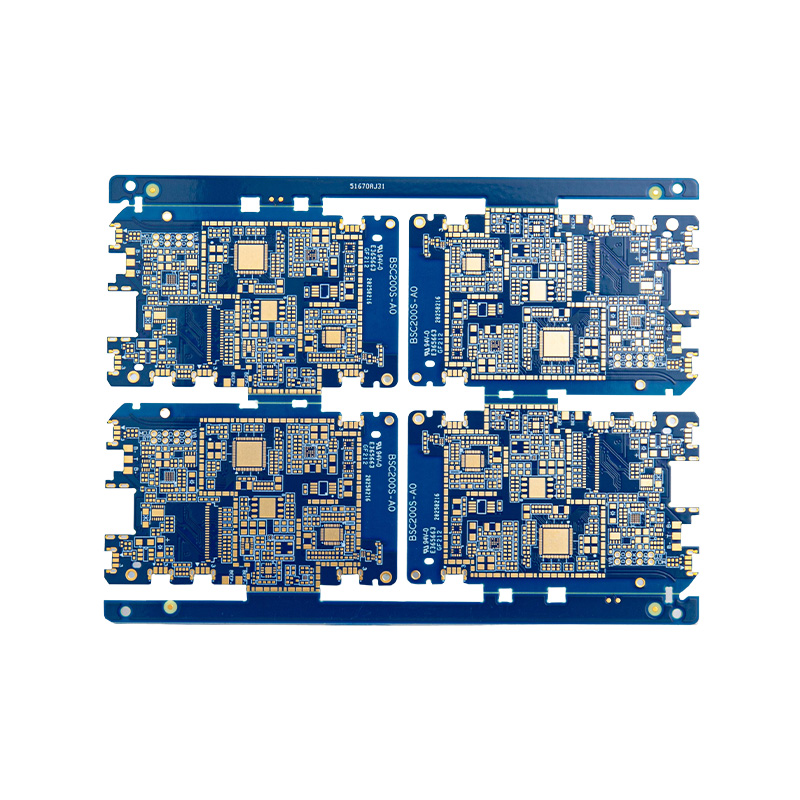

Double-Sided Blue Gold Plating PCB
-
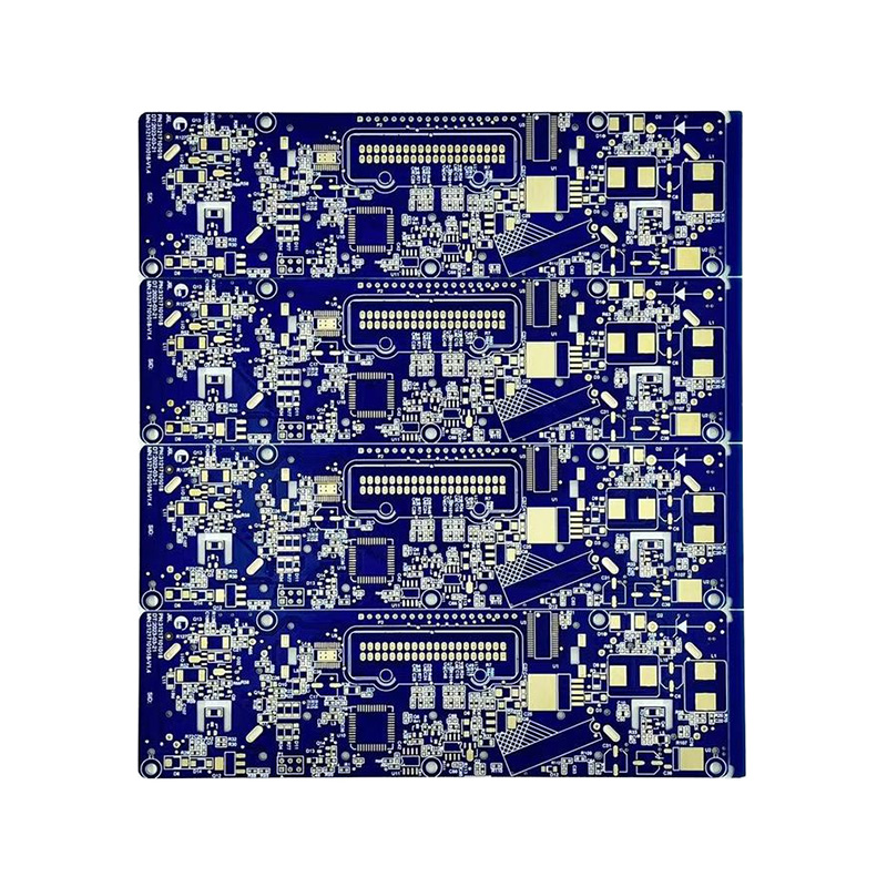
Double-Sided Gold-Plated PCB
-
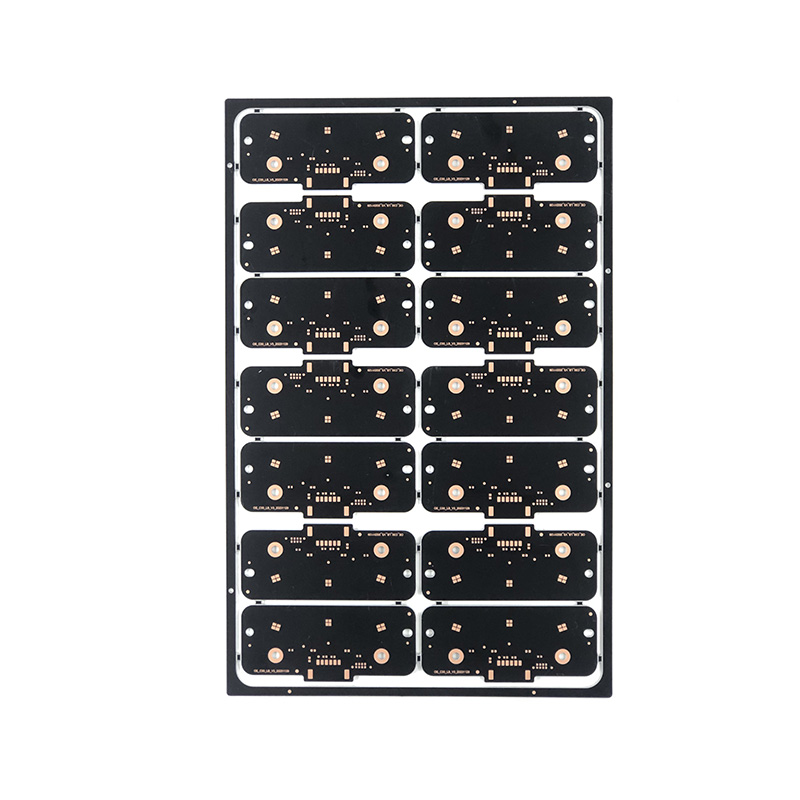
Double-Sided Black 0.3-6Mm OSP PCB Board
-
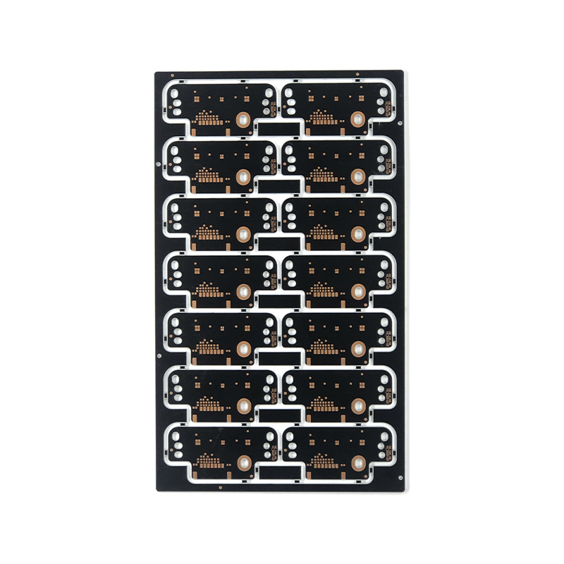
Double-Sided Black High Precision OSP PCB Board
-
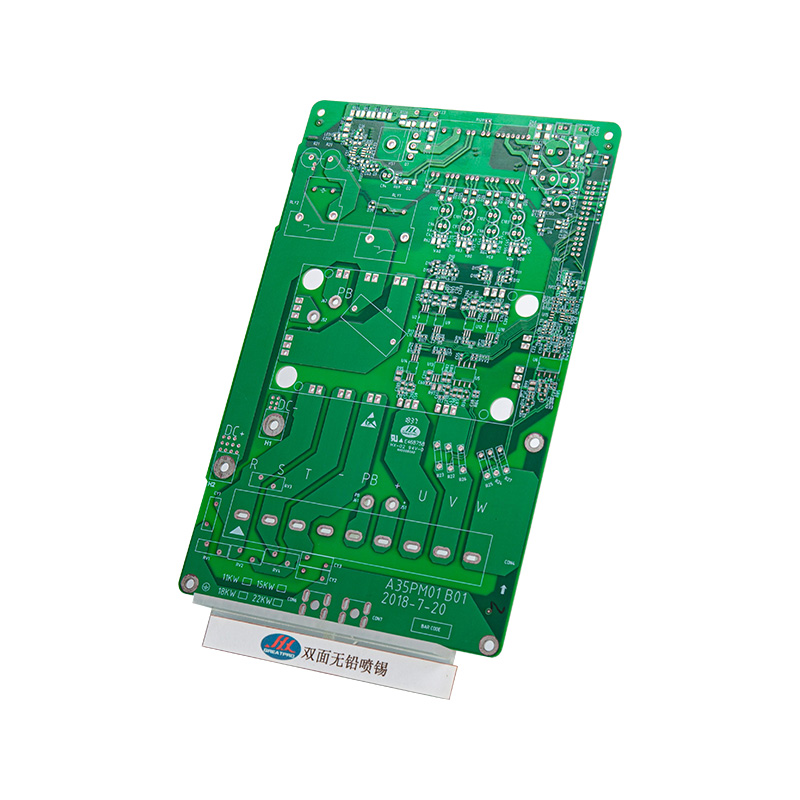
Double-Sided Green Lead-Free Soldered PCB For Power & Automotive Electronics
-
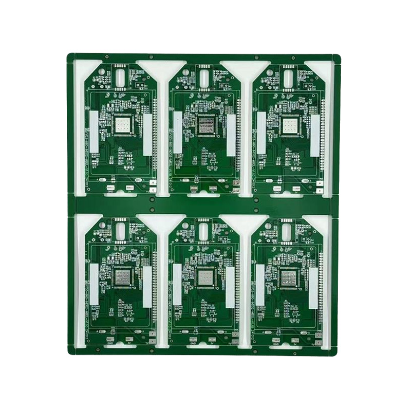
Double-Sided Lead-Free Soldered Green PCB With Enhanced Oxidation Resistance
 LET'S CREATE THE FUTURE TOGETHER

Contact Us Anytime
Copyright © Anhui Hongxin Electronic Technology Co., Ltd. All Rights
Reserved.
privacy
Wholesale Printed Circuit Board Suppliers, Manufacturers

