Ceramic Board
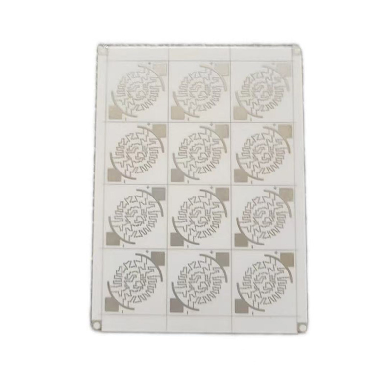
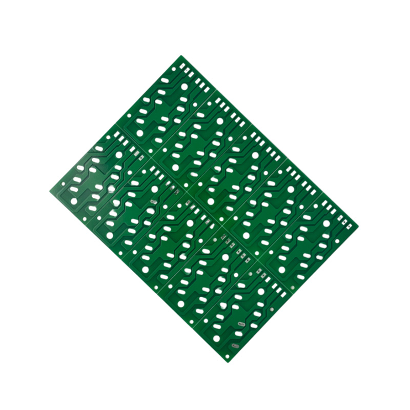
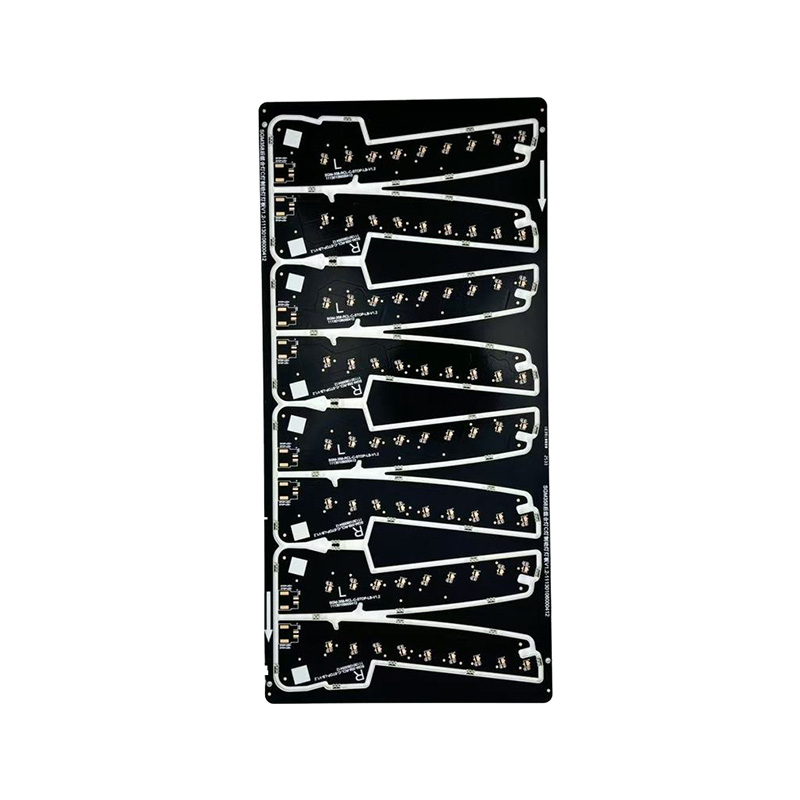
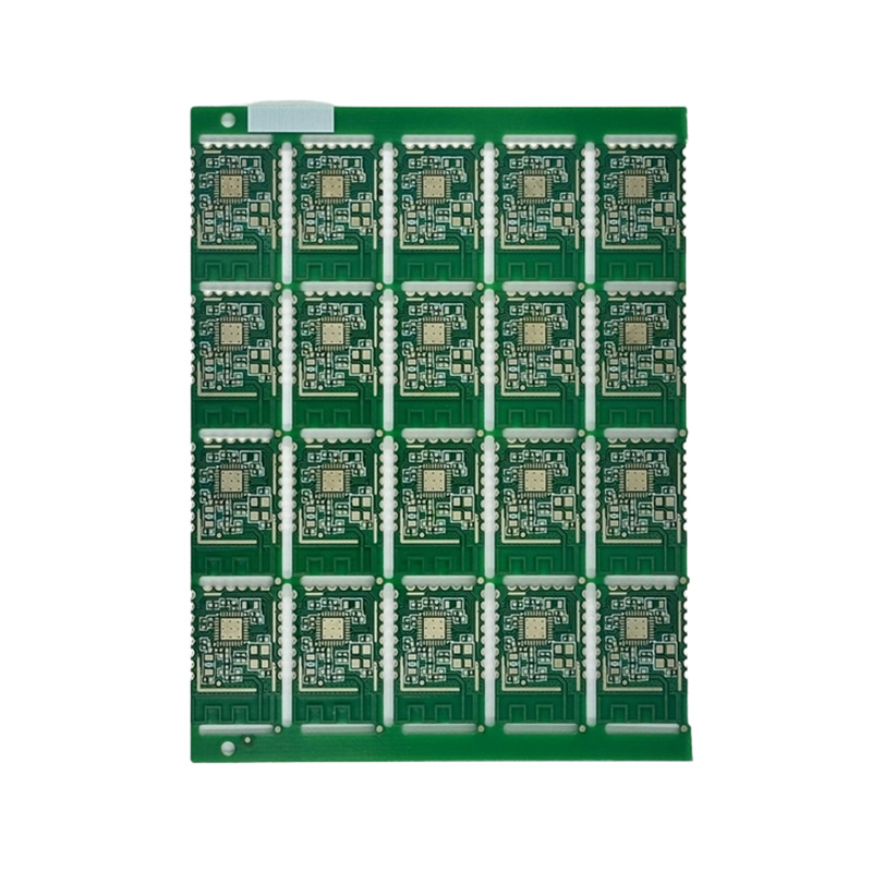
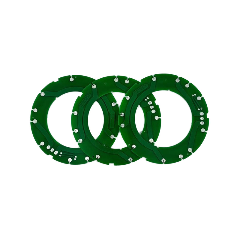
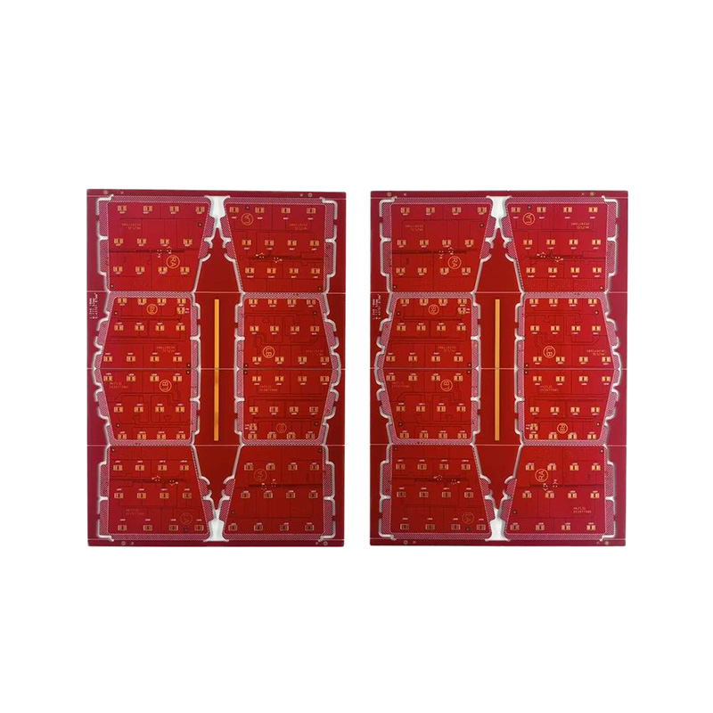
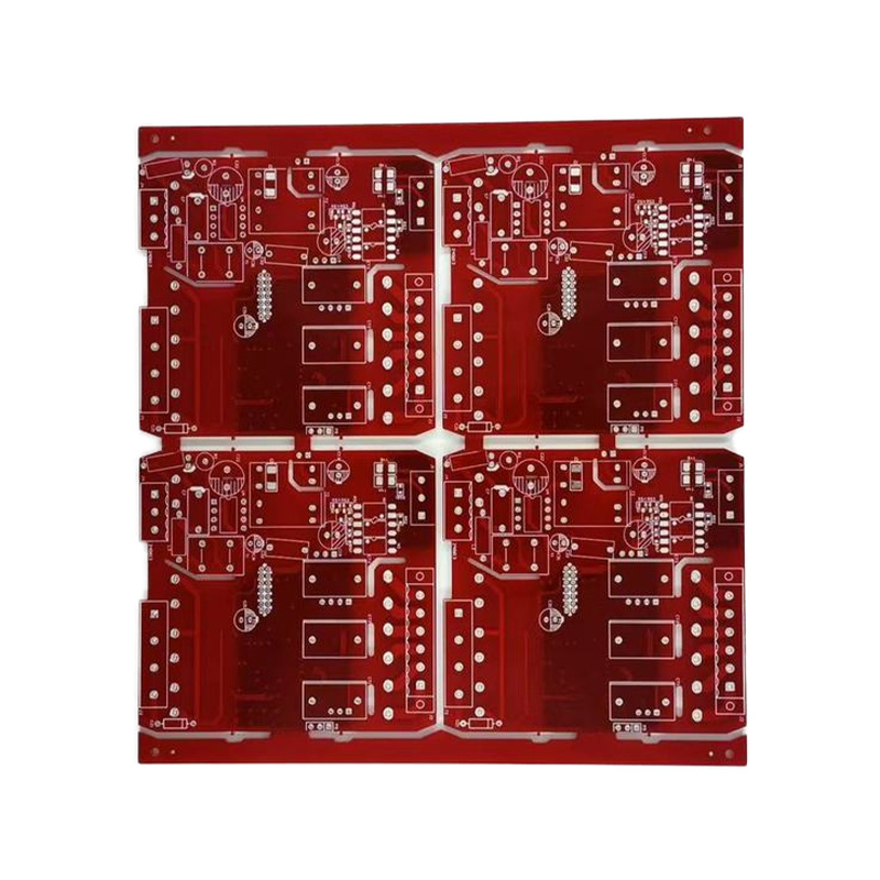
Ceramic PCBs utilize ceramic substrates such as alumina (Al₂O₃) or aluminum nitride (AlN). They boast ultra-high thermal conductivity (15-320W/mK), excellent insulation, and exceptionally high-temperature resistance (capable of withstanding temperatures exceeding 1000°C), making them ideal for applications in extreme environments. Their coefficient of thermal expansion closely matches that of semiconductor chips, effectively addressing the heat dissipation challenges of high-frequency, high-power devices. They are widely used in high-end applications such as 5G communication base stations, aerospace electronics, high-power LEDs, automotive electronics, and medical laser equipment. Ceramic substrates, with their exceptional chemical stability and high-frequency characteristics, demonstrate irreplaceable performance advantages in applications such as millimeter-wave radar and power module packaging, making them a core enabler for the miniaturization and high reliability of high-end electronic systems.
- Specification
- About Hongxin
- Contact Us
|
Materials |
FR-4, aluminum, ceramic, metal, copper, high-frequency, rigid-flex, halogen-free |
|
Board thickness |
0.3-6mm |
|
Copper thickness |
0.5oz-5oz |
|
Layers |
1-32 |
|
Place of origin |
Anhui, China |
|
Surface finish |
Standard HASL, lead-free HASL, OSP, immersion nickel/gold, blue glue, immersion silver, immersion tin |
|
Minimum aperture |
0.25mm |
|
Minimum trace width |
3mil (0.075mm) |
|
Minimum trace spacing |
0.075mm |
|
Board thickness to aperture ratio |
10:1 |


 English
  Español
  Français

