


 English
 Español
 Français

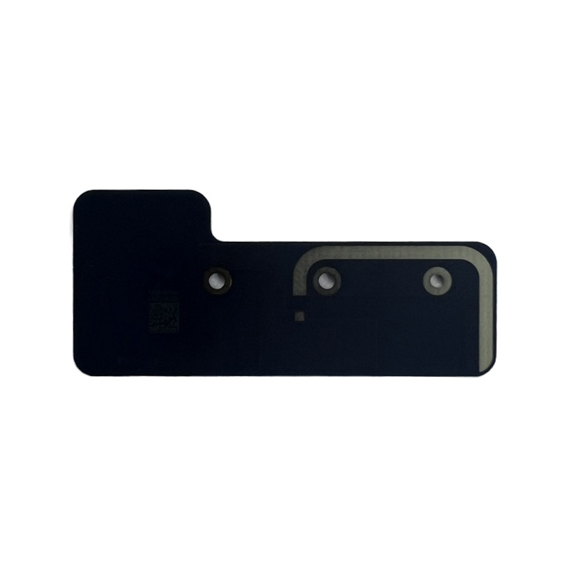
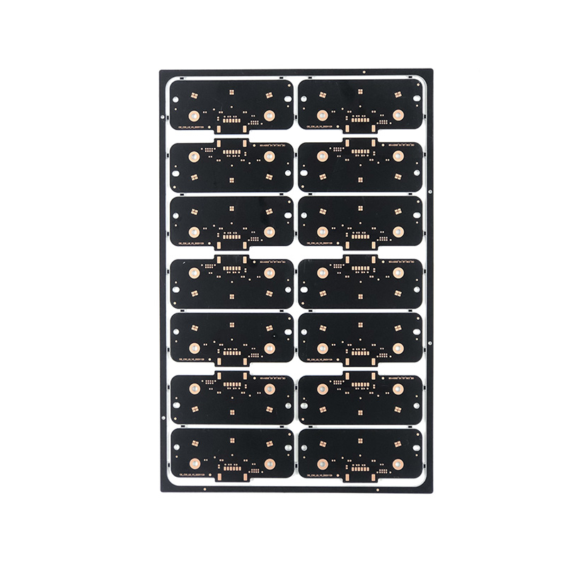
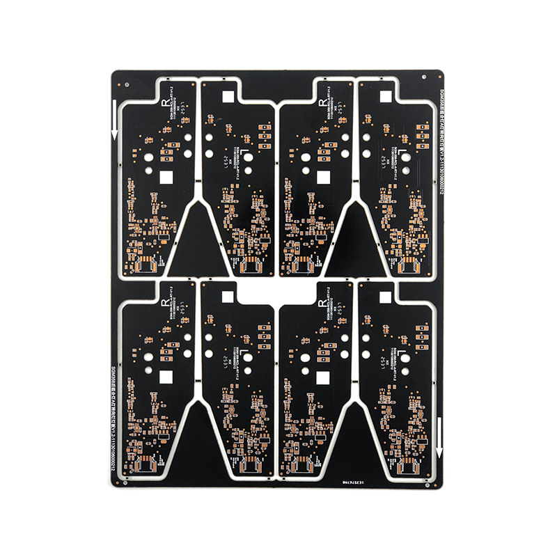
Black High-Frequency PCB
High-frequency PCBs utilize specialized materials with low dielectric constants (Dk) and dissipation factors (Df), such as PTFE and ceramic fillers, to significantly reduce signal transmission loss and latency, ensuring the integrity and stability of high-frequency signals. Their superior impedance control (tolerance ±5%) and temperature stability enable them to excel in high-frequency applications such as 5G communication base stations, millimeter-wave radar, satellite communications, high-speed digital circuits, and RF modules. High-frequency PCBs support ultra-fine line designs (line widths/line spacings up to 50μm) and exhibit excellent anti-interference performance, making them core components for high-speed, high-precision signal transmission in high-end communications equipment, aerospace electronics, and automotive radar systems.
- Specification
- About Hongxin
- Contact Us
|
Materials |
FR-4, aluminum, ceramic, metal, copper, high-frequency, rigid-flex, halogen-free |
|
Board thickness |
0.3-6mm |
|
Copper thickness |
0.5oz-5oz |
|
Layers |
1-32 |
|
Place of origin |
Anhui, China |
|
Surface finish |
Standard HASL, lead-free HASL, OSP, immersion nickel/gold, blue glue, immersion silver, immersion tin |
|
Minimum aperture |
0.25mm |
|
Minimum trace width |
3mil (0.075mm) |
|
Minimum trace spacing |
0.075mm |
|
Board thickness to aperture ratio |
10:1 |
Product Overview
Black High-Frequency PCB is an RF/microwave circuit board built upon low-loss high-frequency substrates with black solder mask. It aims to minimize signal loss and phase delay for high-frequency circuits. Substrate selection, stack-up structure and impedance parameters need to be reviewed against customer Gerber files and target frequency-band requirements.
Typical Applications
- 5G communication infrastructure
- Millimeter-wave automotive radar
- Satellite & aerospace communication
- High-speed digital and RF modules
- Radio-frequency IoT devices
Key Features
- Low Dk / Df substrate reduces RF signal attenuation and preserves signal integrity
- Achievable impedance tolerance down to ±5%; fine trace design down to 50 μm line width / space
- Black solder mask delivers improved heat absorption and higher AOI inspection contrast
- Optimized stack-up structure suppresses crosstalk for microwave-related circuits
- Multiple surface finish options available for RF soldering requirements
FAQ
Q: What substrate choices are available for black high-frequency PCB?
A: Main options cover PTFE, ceramic-filled composite material, and hybrid stack-up combining high-frequency material with ordinary FR4.
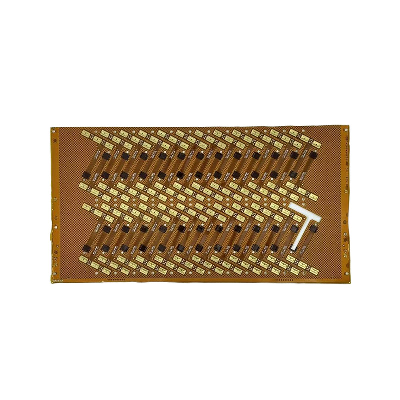
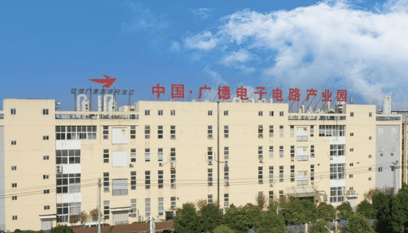
Anhui Hongxin Electronic Technology Co., Ltd. is located in the China PCB Industrial Park, Guangde Economic Development District, Anhui Province. Established in October 2013, our factory occupies 20,000 square meters and employs 110 staff members, including over 7 professional engineers with more than 15 years of experience. The company's PCB products include 1-32 layer boards, high-Tg boards, thick copper boards, rigid-flex boards, high-frequency boards, hybrid dielectric laminated boards, buried via boards, metal-based boards, and halogen-free boards. High-precision PCB rapid prototyping is available, with bulk orders for single- and double-sided boards delivered within 6-7 days, 4-8 layer boards within 9-20 days, 10-16 layer boards within 20-25 days, 16-32 layer boards within 25-45 days, HDI boards within 25 days, and double-sided prototyping deliverable as quickly as 24 hours. We are committed to providing high-quality products and professional services to global customers, and we have the capability to deliver both large quantities and small batches. The surface treatment processes of our products are complete. The base material types include FR-1, 22F, CEM-1, CEM-3, FR-4 (with high Tg, halogen-free, etc.), high-frequency boards, and metal substrates. All product types have passed ISO9001, ISO14001, ISO45001, IATF16949 international quality management system certifications, as well as UL safety certifications. Our sales network extends from inland areas to Southeast Asia, Europe, and America. In the fierce market competition, we have always received high praise from customers.


About
Anhui Hongxin Electronic Technology Co., Ltd.
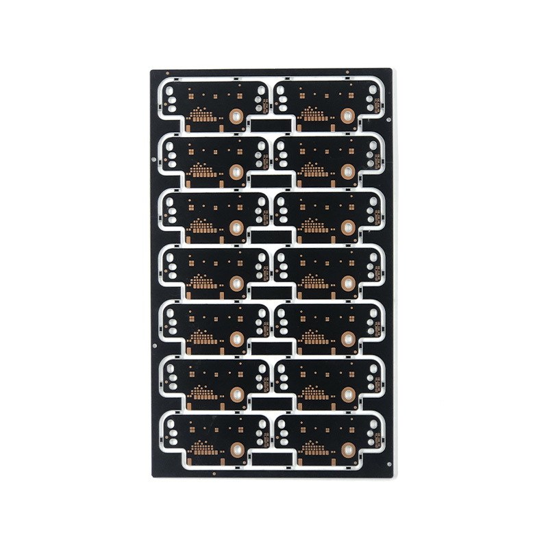
Anhui Hongxin Electronic Technology Co., Ltd. is China Black High-Frequency PCB Suppliers and Wholesale Black High-Frequency PCB Factory. It is located in China P C B Industrial Park, Guangde Economic Development District, Anhui Province. Established in October 2 0 1 3, our factory occupied 8, 413 square meters and employs 110 staff members, including over 7 professional engineers with more than 15 years of experience. The company's P C B products include 1- 32 layer boards, high Tg boards, thick copper boards, rigid-flex boards, high- frequency boards, hybrid dielectric laminated boards, buried via boards, metal-based boards, and halogen- free boards. High-precision P C B rapid prototyping is available, with bulk orders for single and double -sided boards delivered within 6 - 7 days, 4 - 8 layer boards within 9 - 20 days, 10 - 16 layer boards within 20 - 25 days, 16 - 32 layer boards within 25 - 45 days, H D I boards within 25 days, and double- sided prototyping deliverable as quickly as 24 hours.
We are committed to providing high-quality products and professional services to global customers, and we have the capability to deliver orders of both large quantities and small batches. The surface treatment processes of our products are complete. The base material types include FR-1, 22F, CEM-1, CEM-3, FR-4 (with high Tg, halogen-free, etc.), high-frequency boards, and metal substrates. All product types have passed ISO9001, ISO14001, ISO45001, IATF16949 international quality management system certifications and UL safety certifications. Our sales network extends from inland areas to Southeast Asia and Europe and America. In the fierce market competition, we have always received high praise from customers.
Certificate Of Honour


 LET'S CREATE THE FUTURE TOGETHER

Contact Us Anytime
Copyright © Anhui Hongxin Electronic Technology Co., Ltd. All Rights
Reserved.
privacy
Wholesale Black High-Frequency PCB Suppliers, Factory

Message
We are committed to providing high-quality products and professional services to global customers
