Balancing Signal Integrity, Power Distribution, and Impedance in Multilayer PCB Stack-up Design
The Importance of a Scientific Stack-up Design
In high-speed electronic design, the configuration of layers in a Multilayer PCB is the foundation for electrical performance. A scientific stack-up does more than just organize traces; it acts as the primary defense against Electromagnetic Interference (EMI) and ensures stable power delivery.
- Signal Return Path Management: By placing signal layers adjacent to solid ground planes (GND), we ensure the shortest possible return path. This reduces loop inductance and significantly lowers EMI radiation.
- Impedance Control: Precise control over the thickness of the dielectric material (Prepreg and Core) and the trace width allows for consistent characteristic impedance (e.g., 50Ω single-ended or 100Ω differential), which is critical for high-speed data transmission.
- Power Decoupling: Placing power (VCC) and ground planes in close proximity creates plane capacitance, which helps filter high-frequency noise and stabilizes the Power Delivery Network (PDN).
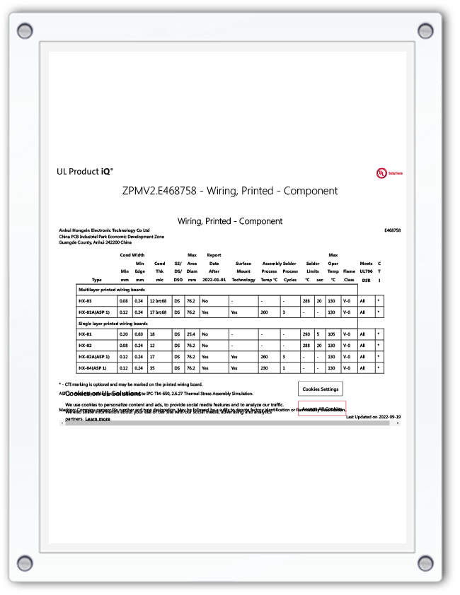
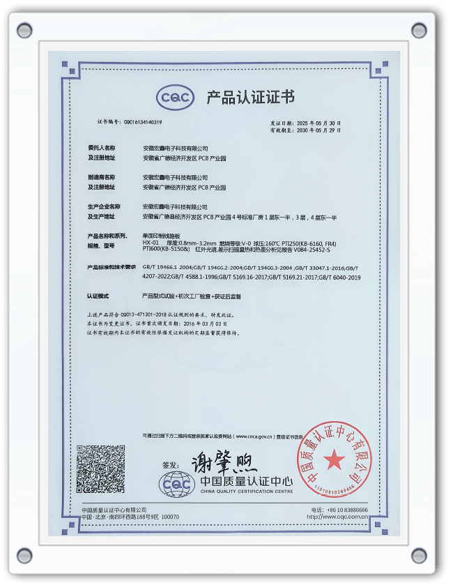
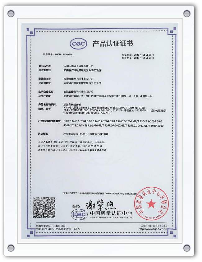
Anhui Hongxin Electronic Technology Co., Ltd., located in the China PCB Industrial Park in Guangde, brings over a decade of expertise to complex multilayer projects. Our facility covers 20,000 square meters and is managed by a team of professional engineers with over 15 years of experience. We specialize in producing boards from 1 up to 32 layers, utilizing advanced materials like high-Tg FR-4, high-frequency laminates, and hybrid dielectric structures to meet the most demanding stack-up requirements.
Technical Parameter Comparison: Standard vs. High-Performance Multilayer PCBs
Selecting the right parameters is essential for balancing cost and performance. Below is a comparison of typical specifications handled by our engineering team:
| Feature |
Standard Multilayer PCB |
High-Precision Multilayer (Hongxin) |
Design Benefit |
| Layer Count |
4 - 8 Layers |
Up to 32 Layers |
Supports ultra-high density routing |
| Impedance Tolerance |
±10% |
±5% (Strict Control) |
Ensures signal integrity for high-speed I/O |
| Min. Dielectric Thickness |
4 mil |
2.5 mil |
Stronger capacitive coupling for PDN |
| Via Technology |
Through-hole only |
Blind & Buried Vias / HDI |
Reduces parasitic capacitance and saves space |
| Registration Accuracy |
±3 mil |
±1.5 mil |
Prevents interlayer misalignment in high-layer counts |
Frequently Asked Questions (FAQ)
Q1: How does Anhui Hongxin Electronic Technology Co., Ltd. support rapid prototyping for complex multilayer designs?
We understand that time-to-market is critical. Anhui Hongxin Electronic Technology Co., Ltd. offers high-precision rapid prototyping services. We can deliver 4-8 layer boards within 9-20 days, and even for highly complex 16-32 layer boards, we maintain an efficient window of 25-45 days. Our streamlined design-to-production workflow, backed by ISO9001 and IATF16949 certifications, ensures that speed never compromises quality.
Q2: What materials does Anhui Hongxin Electronic Technology Co., Ltd. use for high-frequency or high-temperature applications?
Our material inventory is extensive to suit various industrial needs. Anhui Hongxin Electronic Technology Co., Ltd. utilizes base materials including FR-4 (High Tg and Halogen-free), high-frequency laminates for RF applications, and metal substrates for thermal management. We also offer hybrid dielectric laminated boards, which allow customers to combine different materials in a single stack-up to optimize both cost and high-frequency performance.
Q3: Can Anhui Hongxin Electronic Technology Co., Ltd. handle both small batches and large-scale global orders?
Yes. With a factory of 20,000 square meters and 110 dedicated staff, Anhui Hongxin Electronic Technology Co., Ltd. has the versatile capability to deliver both small R&D batches and large-scale production quantities. Our sales network already extends across Southeast Asia, Europe, and America, supported by UL safety certifications and a commitment to professional service that has earned us high praise in the global market.


 English
  Español
  Français