Optimizing EMI Reduction and Thermal Distribution in Double-sided PCB Design
Strategies for EMI Reduction and Signal Integrity
In a Double-sided PCB, the limited layer count makes electromagnetic interference (EMI) management a priority. Unlike multilayer boards with dedicated ground planes, a double-sided design requires strategic routing to maintain signal integrity.
- Loop Area Minimization: Routing signal traces directly above a return path on the opposite layer helps minimize the loop area, which is the primary source of radiated EMI.
- Orthogonal Routing: To prevent crosstalk, traces on the top layer should run perpendicularly to those on the bottom layer.
- Ground Pouring (Copper Flood): Filling unused areas with copper and connecting them to the ground (GND) via stitching vias creates a pseudo-shielding effect.
Thermal Distribution and Management
Effective heat dissipation in a Double-sided PCB relies on the intelligent use of copper and substrate selection. Balancing the thermal load prevents localized "hot spots" that can lead to component failure or board warping.
- Thermal Vias: Placing vias under high-power components facilitates heat transfer from the top layer to the bottom layer, utilizing the surface area of both sides for cooling.
- Thick Copper Technology: Using thicker copper foils increases the thermal conductivity of the traces themselves.
- Symmetry in Copper Distribution: Ensuring a balanced copper density between the top and bottom layers prevents the board from bowing or twisting during reflow soldering.
Anhui Hongxin Electronic Technology Co., Ltd., located in the China PCB Industrial Park, Guangde, has been a leader in high-precision PCB manufacturing since 2013. With over 20,000 square meters of production space and a team of professional engineers with 15+ years of experience, we specialize in everything from 1-32 layer boards to high-Tg and metal-based substrates. Our expertise ensures that even complex double-sided designs are optimized for both thermal and electrical performance.
Parameter Comparison: Standard vs. Optimized Double-sided PCB Design
The following table illustrates the technical differences between basic designs and high-performance boards optimized by professional engineering teams:
| Technical Parameter |
Standard Double-sided PCB |
Optimized Design (Hongxin Standards) |
Impact on Performance |
| Base Material Tg |
Standard FR-4 (130°C) |
High-Tg FR-4 (>170°C) |
Better stability at high temperatures |
| Copper Thickness |
0.5oz - 1.0oz |
2.0oz - 6.0oz (Thick Copper) |
Higher current capacity and heat dissipation |
| Min. Trace Width/Spacing |
6 / 6 mil |
Down to 3 / 3 mil (High Precision) |
Enables denser, complex circuitry |
| Via Connection |
Standard PTH |
Buried Via / Thermal Via Arrays |
Enhanced vertical heat and signal transfer |
| Prototyping Lead Time |
3-5 Days |
As fast as 24 Hours |
Accelerated R&D cycles |
Frequently Asked Questions (FAQ)
Q1: How does Anhui Hongxin Electronic Technology Co., Ltd. ensure the quality of high-precision double-sided boards?
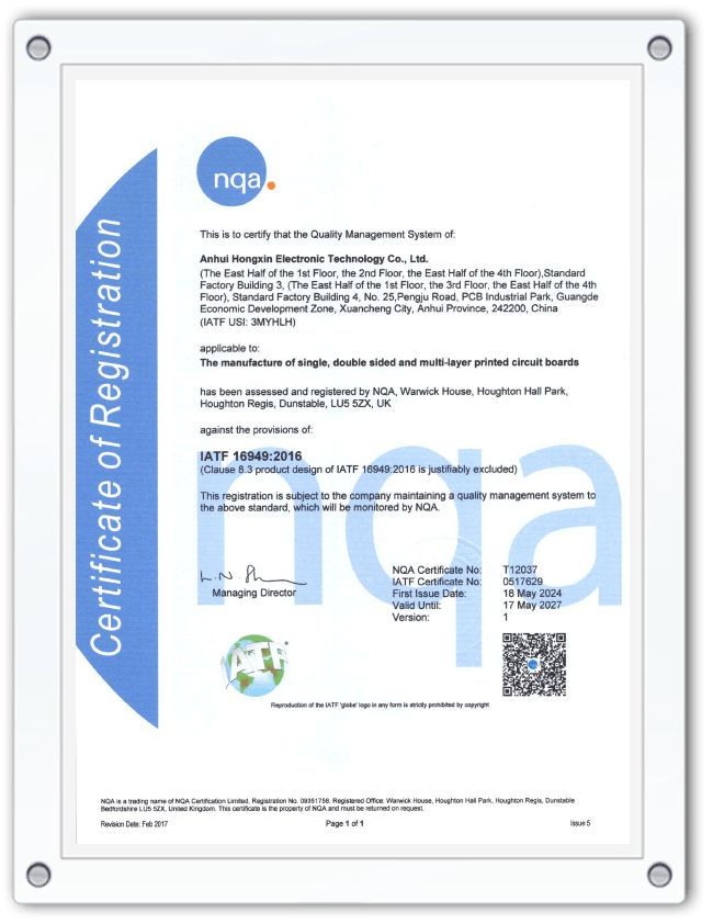
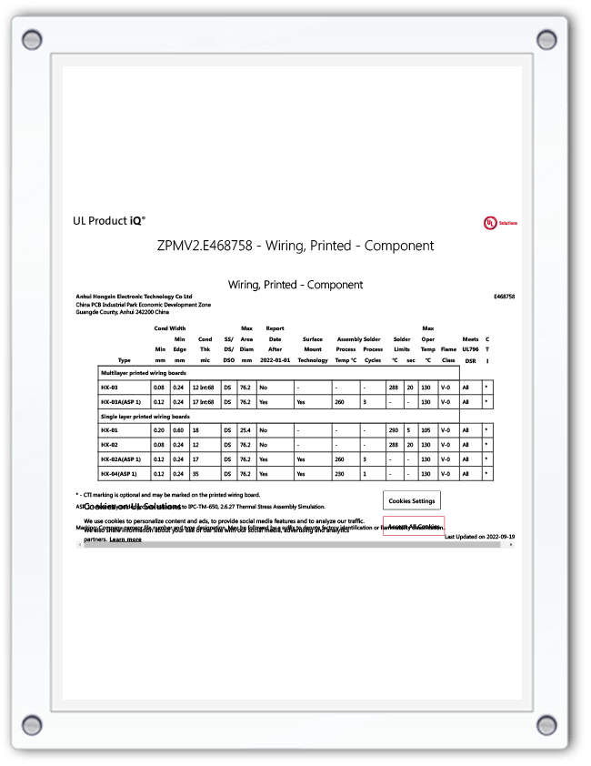
Quality is at the core of Anhui Hongxin Electronic Technology Co., Ltd. Our production processes have passed international certifications including ISO9001, IATF16949 (Automotive Quality), and UL safety certifications. Every board, whether a rapid prototype or a bulk order, undergoes rigorous testing to ensure it meets our high-precision standards, giving our global customers in Southeast Asia, Europe, and America total peace of mind.
Q2: What options are available for specialized double-sided applications, such as high-power or high-frequency devices?
Anhui Hongxin Electronic Technology Co., Ltd. offers a wide range of substrate materials including high-frequency boards, metal substrates (for extreme cooling), and halogen-free boards. Our engineers, boasting over 15 years of industry experience, can assist in selecting the right dielectric and copper weight to ensure your double-sided board survives fierce market competition and technical demands.
Q3: How fast can Anhui Hongxin Electronic Technology Co., Ltd. deliver double-sided prototypes and bulk orders?
We pride ourselves on our rapid response capabilities. Anhui Hongxin Electronic Technology Co., Ltd. can deliver double-sided PCB prototyping as quickly as 24 hours. For bulk orders, we maintain a highly efficient 6-7 day delivery window for single- and double-sided boards. This speed, combined with our 20,000 sqm facility and 110 dedicated staff members, allows us to handle both large-scale production and small-batch rapid prototyping with ease.


 English
  Español
  Français