Communication PCB: The Core Foundation Supporting Stable High-Speed Communication Systems
With the rapid development of 5G communication, data centers, optical modules, routing and switching equipment, and industrial communication systems, Communication PCBs are no longer simple electrical interconnection carriers. They play a critical role in determining signal integrity, system stability, and long-term reliability.
Communication PCBs are required to meet multiple demanding technical standards at the same time, including high speed, high frequency, high density, and high reliability. This places much higher requirements on material selection, stack-up design, impedance control, and manufacturing processes.
Key Technical Characteristics of Communication PCBs
Compared with consumer electronics or general industrial PCBs, Communication PCBs typically have the following characteristics:
| Technical Aspect |
Core Requirements |
| Signal Speed |
Support for high-speed and ultra-high-speed signal transmission (Gbps level) |
| Impedance Control |
Strict single-ended and differential impedance tolerances |
| Material Performance |
Low dielectric constant (Dk) and low dissipation factor (Df) |
| Layer Structure |
Multi-layer, HDI, and buried/blind via structures are common |
| Thermal Stability |
High Tg and strong resistance to thermal shock |
| Long-Term Reliability |
Designed for 24/7 continuous operation environments |
Because of these features, Communication PCBs are widely used in:
- 5G / 4G base stations and small cell equipment
- Optical communication modules, switches, and routers
- Data center servers and high-speed backplanes
- Industrial communication control systems
- Network security and communication terminal devices
High-Frequency and High-Speed Requirements: Material Selection Matters
The stability of communication performance depends heavily on the base material system. In practical applications, common material solutions include:
| Material Type |
Typical Applications |
| High Tg FR-4 |
Mid-speed and high-speed communication equipment |
| Low-loss high-frequency materials |
RF and microwave communication systems |
| Hybrid dielectric laminates |
Mixed high-speed digital and RF designs |
| Metal-based boards |
High-power communication modules with thermal requirements |
| Halogen-free materials |
Markets with strict environmental and safety regulations |
In communication PCB manufacturing, material stability and batch consistency are especially critical. This is one of the core capabilities that distinguishes professional communication PCB manufacturers.
With comprehensive coverage of 1–32 layer boards, high-frequency PCBs, rigid-flex boards, hybrid dielectric laminates, as well as fast prototyping and volume production capabilities, Anhui Hongxin Electronic Technology Co., Ltd. is well positioned to support communication equipment customers from R&D to mass production.
Manufacturing Process Requirements for Communication PCBs
Communication PCBs demand much higher manufacturing standards than ordinary PCB products, mainly reflected in:
- High-precision imaging and etching control
- Accurate layer-to-layer alignment for multi-layer boards
- Strict impedance testing and process monitoring
- Stable plated through-hole and via metallization quality
- Complete and reliable surface finishing processes
Only manufacturers with mature capabilities in multi-layer, high-frequency, and HDI PCB production can consistently deliver stable performance for communication PCB projects.
Typical Technical Parameters for Communication PCBs
| Item |
Common Range |
| Layer Count |
4–32 layers |
| Board Thickness |
0.4–3.2 mm |
| Copper Thickness |
1–6 oz (customizable) |
| Impedance Tolerance |
±5% or tighter |
| Surface Finish |
ENIG, OSP, Immersion Tin, Immersion Silver, etc. |
| Certifications |
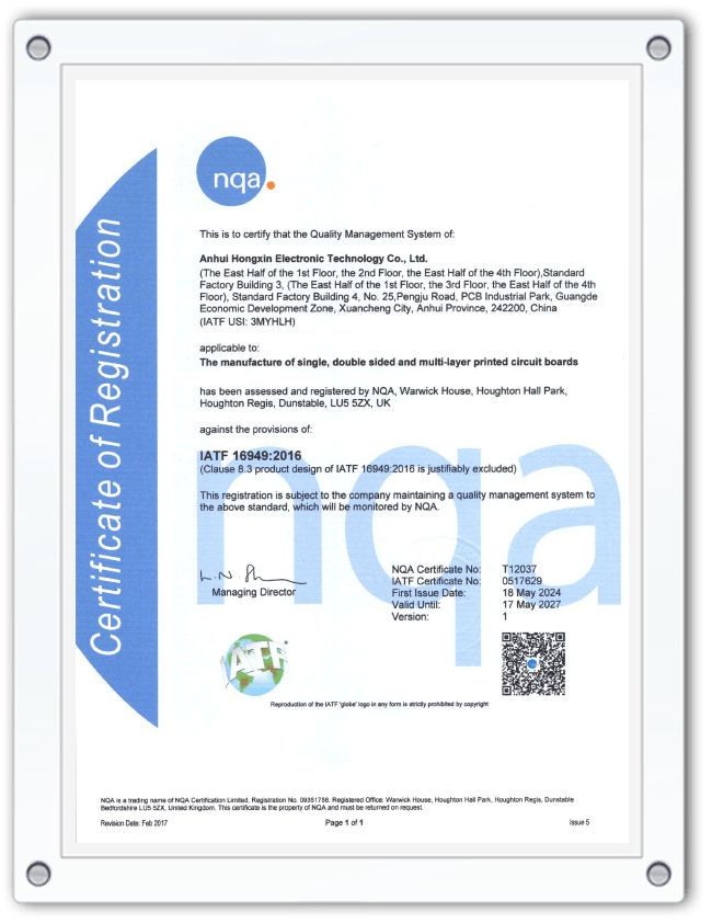
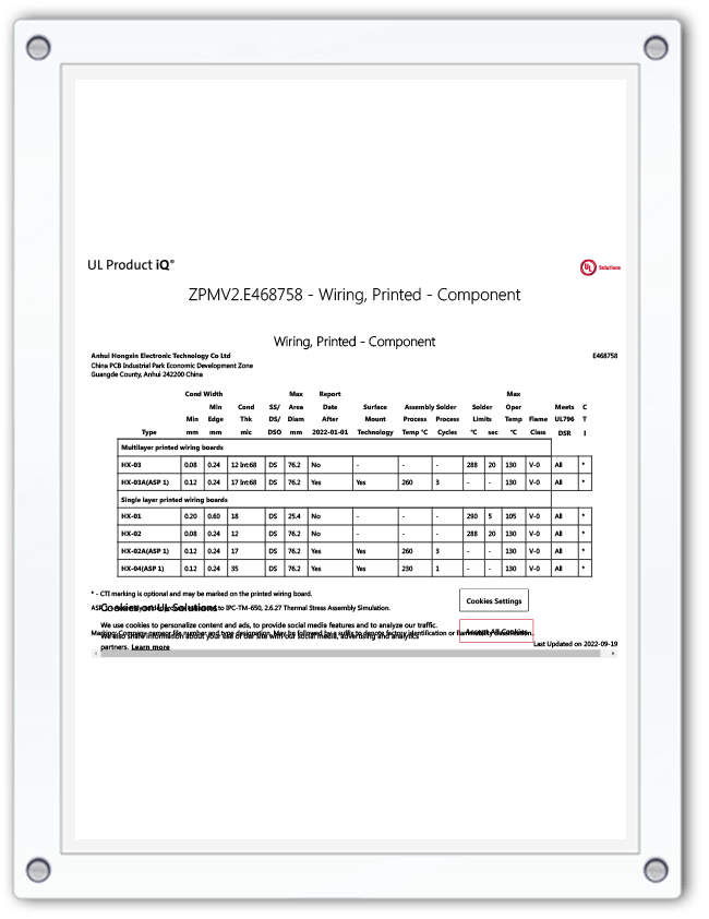
ISO, IATF, UL, and other international standards |
Communication PCB FAQ
Do communication PCBs always require high-frequency materials?
Not necessarily. The choice depends on signal frequency, transmission distance, and system design. Many high-speed digital communication applications can still use high Tg FR-4 or hybrid stack-ups to balance performance and cost.
What is the typical lead time for multi-layer communication PCBs?
Lead time varies depending on layer count and process complexity. Manufacturers with mature production systems can provide fast turnaround for prototypes and small-to-medium batches, helping customers shorten development cycles.
Why is impedance control so important for communication PCBs?
High-speed signals are extremely sensitive to impedance variations. Poor impedance control can cause signal reflection, crosstalk, and eye diagram degradation, directly affecting communication quality and system stability.
Are communication PCBs suitable for small batch production and rapid prototyping?
Yes. Communication equipment development often requires multiple design iterations. Manufacturers that support high-precision rapid prototyping and scalable volume production offer significant advantages.
Choosing the Right Communication PCB Manufacturer
As communication technology continues to evolve toward higher speed, higher frequency, and higher integration, Communication PCBs have become a fundamental guarantee of system performance.
From material systems and process capabilities to quality certifications and delivery stability, selecting a manufacturer with proven communication PCB experience can significantly reduce project risks and improve overall product competitiveness.
If you are looking for stable, scalable, and communication-focused PCB solutions, working with a professional communication PCB manufacturer is a strategic choice.


 English
  Español
  Français